Let's start with the Technical (built my own 2-pin electronic blinker for 3W ~ 300W for my Div900 years ago - if that helps):
Your setup isn't safe enough if you want to be assured of use of your indicators at all times. Which you do.
Why not? Because of the following reasons:
- The 78x05 type regulators are hardly ever specified for high-transients (supra-40V), nor are they guaranteed to perform correctly for negative input, while not as likely as it was in 1960's cars, it's not impossible and broken is broken.
- Similarly you want your opto-couplers protected from inversion by an extra, at least 100V capable diode. Nor do you want one switch to turn on another in vehicles, if you do it properly, so adding more 4148's to the other inputs seems best. (Your forward current at 30V seems to stay below limits, so that seems ok).
- Your MOSFETs are Connected the wrong way around. They show P-Type, but their source is connected to the low-side load. This means your lights are always on.
- How do your MOSFETs turn off (once you have flipped them)? There should be a pull-up to their gates, or your lamps will turn on and then maybe, once, in the distant future through leakage turn off.
- Be aware (when you start debugging) that your MOSFETs are connected directly to the dirty voltage, and though it's much less likely to be problematic, there's a chance when pull-up's are there some noise may filter back in. I've never had trouble with that myself with AVRs though, as their output stages are rock solid. If you do use an Opto-Coupler there, beware to calculate the drive currents and turn/on turn off times, you may still need an extra transistor there.
- Your base resistors for your NPNs can be a factor 10 larger, this will still switch exceptionally well, but it's not mandatory (though I'd do it - for the current consumption).
- Without any extra capacitance that 22 Ohm on your Vcc will only make your MCU more susceptible to supply noise that's coupling in. Any switching current to its core will need to go through 22 Ohm + Board inductance without any nearby help.
- Not so much a problem, but a tip: Make sure you hook the power wire up to something that doesn't turn on in any setting you don't want it on in. Since you estimate a pretty appreciable steady-state current use by your relay. Some bikes (mine included) power the indicators by default in more settings than just the one where you're driving / running the engine.
So, think about the points above and then I suggest you also put in an input-clamp, that clamps a while before any component hits their limit.
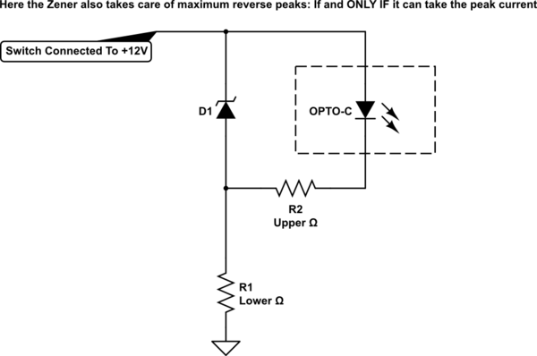
You can consider splitting the opto-coupler resistance in two parts, if you want full protection, and protect the upper half + diode with a 15V zener. If you have that zener and a 350-ish Ohm resistor in the protected chain, you're certain the LED will not see more than a 40mA share. If you do, though, do use a decent zener, not one of those 0402 grains of salt, in case spikes come often and close together those will evaporate just as happily as your couplers. I don't expect it to be needed, but it'd look like this:

simulate this circuit – Schematic created using CircuitLab
You can add some more filtering on supply leading only to your regulator as well, since you seem to be sticking to the bare minimum. The blinker cutting out once every few seconds isn't that harmful if you blink at standard 1.5Hz-ish rate, but if it happens every 10ms you may not be blinking all that much, ever.
Also, be aware that with no or low inductance, 300nF does nearly nothing to compete with very heavy switching loads and sources in your system. They laugh at anything expressed in nanos. Unless you choose a 0.05mm2 wire to power the set-up... In which case even LED lights turning on will make your relay reset.
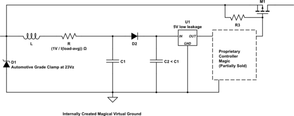
What I did myself was a well calculated version of this:

simulate this circuit
This isn't Ideal, as your clamp is in a high-current path, and who knows. It'd have been better encapsulated in a somewhat safer frame with a limited current. But I wanted to also offer some protection to the down-stream LED lights, as they were ready-made after-market back then, and those lights are teh poop with safety. Hence also the need to not dampen too much, for fear of having to swap in a 21W regular along the side of the road. These days almost everything on the bike is home made or maintained, so some tweaks would be possible, had I not encased it in military grade resin.
C2 is (much) smaller than C1, because you want the filter effect to be verifiably stronger than the boost effect. If the main body of capacitance is C2, you are potentially building a boost converter powered by your alternator frequency.
R is dampening for unwanted effects, such as the boost work or oscillations at unexpected frequencies, and it doesn't hurt in front of a linear regulator anyway.
My regulator was low-leakage as my MCU spends most of its life (even while blinking) in a sub 1uA sleep, having 3mA drain by the regulator would have been a point of great :'(.
L and C1 are selected for a good filtering responses at the frequencies expected in your device at realistic drains from the regulator. For frequency my suggestion is to aim at 35Hz to 2.5kHz for most Touring/Sport-Tour Bikes and up to 5kHz for Sport and SuperSport (peak-RPM/60 * 3 * 7-ish). Where obviously the higher frequencies should only come in when you see if you're not creating any unwanted oscillations anywhere.
If you can get it so that C2 is still at least 100nF and C1 is at least 10 times that, or 25 times... That's where at my lab the scope and the bike meet, to see how well my guesstimation worked.
Of course, all parts between a positive voltage and ground in my design were chosen for low leakage as well, as in all my automotive/bike-o-motive designs.
(Mind you, none of the above contains any maths other than quick top-of-head)
And one more note, before the comments come in: Of course I should remove the point about the virtual magic ground, as with a true virtual ground the TVS wouldn't work, etc etc, but I wanted to show off a little for the hours of typing and putting up with the circuit editor. In reality the TVS is even more cleverly placed, but that'd give away some parts I signed away inside the dotted box.
Then, I would like to add a little off-topic, since you brought it up yourself;
Be aware that several, if not many, calamity professionals in west Europe, NL especially (my home too), strongly suggest you not use emergency lights in between traffic. It causes confusion (to those only seeing one of your sides) as well as aggravation. It hurts more than it helps. While not on-topic as a comment, I felt I should let you know, since confusion and aggravation are leading causes for car drivers to collide with motorcyclists. Just use your headlight, patience and navigational skill.
To date I have spent many hundreds of hours in traffic jams and my "calamity indicator" has been on for a total I estimate below 120minutes, the bulk of which when a screw in my tyre forced me to park "unsafely".
Brief responses to your added questions:
For longer work, you'll have to aim more at new questions, this shouldn't become a complex state-full thread themed "Help Sjoerd finish his design from start to finish"
- The main reason I wouldn't use the 78-types is the high current it draws itself, it can be protected sufficiently by a TVS and a filter. It may be wise for a 24V design to find something a bit more in the direction of 40Vmax, to allow you vehicle voltage to fluctuate upto at least 34V before your protection starts clamping.
1b. Those TVS should work, but make sure you get their clamping voltage a ways beyond your maximum expected normal use voltage, but at least a few volts below the lowest Vmax of your electronics. Try to think about elements that limit the peak pulse to, or preferably way below, 40A. You can use a polyfuse, or the added filter-damping fuse for that.
- It should be fine without opto's, if you have a nice noise source you can stress test it in-lab. A drill driving a medium-size DC motor with a low-voltage source in series might give you a nice worst-case test signal. Or it might not.
- The transistors switch in a sense when you let them saturate. With 4.7k they should be able to pull much more than 70mA and still saturate, when the resistors are connected to a 5V signal. If you want more details there's a lot about that on this site.
- You can add a small resistor as a sort of extra filter, with or without a ferrite bead for the high frequency stuff. But that will require extra capacitance. It is smart to add a 22nF to 100nF bypass capacitor to any digital chip, to supply switching currents locally. There's also a lot about this on this website. Adding a current-limiting resistor to an MCU is a very strange practise. Especially for 200mA on a Tiny45. If your Tiny45 is pulling an average current of 200mA it's broken and your relay can be discarded anyway. Digital chips, if not filtered, get connected directly, because "we" trust them to behave. Unless we know otherwise.
Input filtering and all that:
The capacitors and the inductor in that image get calculated to filter at the appropriate points without causing oscillations. This post is already too long to detail that, but again, there's a lot on filter design on this website already anyway. The reason I mention the C2 to C1 relationship is that if you don't stick to that, there's a risk you are building a boost converter using your alternator ripple, which might boost the voltage to 1.5x, 2x, or even more. This is not the likeliest thing to happen if you're experienced, but when starting out, it's best to stick to the rule for C1 and C2.
The diode is protection from ms-scale cut-outs and input voltage reversal. To note, as well, that if input reversal is a likely possibility, it's best to have all caps before the diode be ceramic or other bipolar types. For longevity.
For the caps you can over-do it, costing money and space and possibly creating high inrush currents, or possibly the opposite: High ESR in the caps, which would dampen the filter even more than the dampening resistor. If you move the dampening resistor before the TVS, when the TVS only protects your electronics, the filter will work better, you can then also look into pi-filtering, but you can also over-do filters quite easily. A simple L-C filter in the ballpark, a small safety resistor and a TVS should get you so close to Automotive spec that it'll probably do well without actual full testing for all but commercial production runs.


