9
\$\begingroup\$

Take a look at this evaluation board for a variable gain RF amp (datasheet): All DC lines have thee caps in parallel, each of a different size
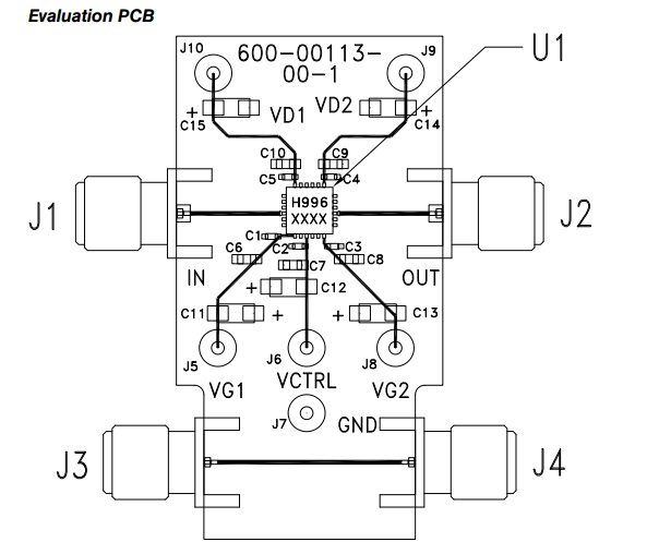
J5-J10 are intended to connect to DC power (with the exception of J6, which is a DC analog control voltage). All of these lines have three capacitors in parallel. Take the trace connected to J10, for example. On your way from J10 to the pin on the chip, you go through these three capacitors:

  • A 2.2 µF capacitor in a big package (called "CASE A" in the datasheet)
  • A 1000 pF capacitor in an 0603 package
  • A 100 pF capacitor in an 0402 package

Why are three parallel caps used instead of one 3.3 µF cap? Why do they all have a different package size? Is the order important (i.e. is it important that the smallest-value capacitors be closer to the chip?

\$\endgroup\$
0

2 Answers 2

24
\$\begingroup\$

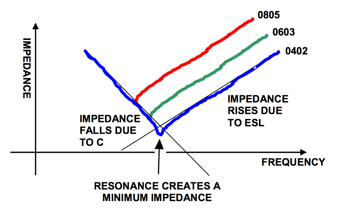
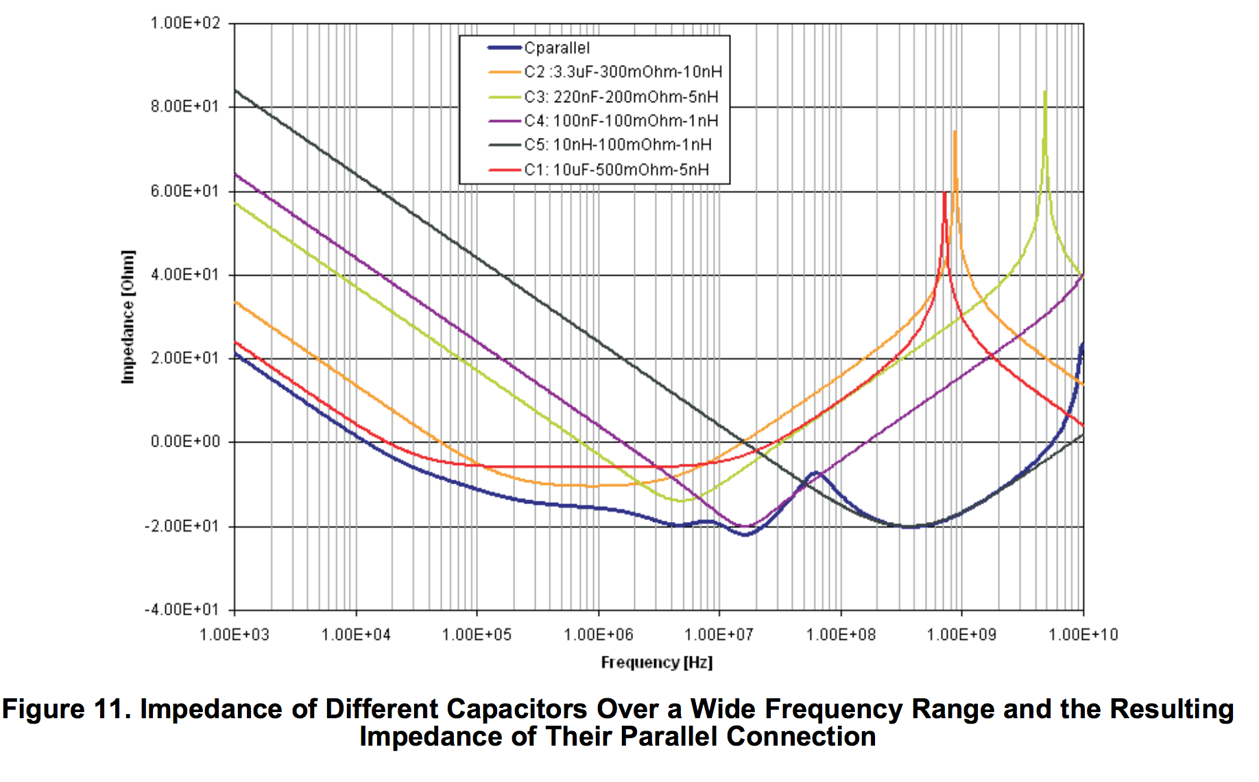
Given a dieletric type, the smaller the capacitor, typically less parasitic inductance it will have (better response at higher frequencies), but also less capacitance. You can mix sizes, values and types of capacitors to achieve a required response that is broader than what a single one can provide. It's not just about the capacitance value.

These images sum it up pretty well:

enter image description here

From "EEVblog #859 - Bypass Capacitor Tutorial".

And

enter image description here

From "Intersil - Choosing and Using Bypass Capacitors - AN1325"

enter image description here

From "TI - High-Speed Layout Guidelines"

\$\endgroup\$
5
  • 5
    \$\begingroup\$ Dave is really happy that you answered this question. So am I \$\endgroup\$
    – Mahkoe
    Commented May 12, 2017 at 15:50
  • \$\begingroup\$ I posted it as a comment but I really had to add as an answer to use that frame. :D \$\endgroup\$
    – Wesley Lee
    Commented May 12, 2017 at 15:54
  • 3
    \$\begingroup\$ Do the capacitors the last plot ("Figure 11") really have a minimum impedance of minus 2 Ohm?! \$\endgroup\$
    – Fritz
    Commented May 12, 2017 at 19:58
  • 3
    \$\begingroup\$ @Fritz, since the plot has the shape of a standard log-log plot, it may be that the Y axis was mislabeled. My guess is that it's NOT "Impedance [Ohm]", but dB instead. \$\endgroup\$ Commented May 13, 2017 at 7:28
  • \$\begingroup\$ Does the kink at the lowest impedance value have any significance for the design engineer? \$\endgroup\$
    – quantum231
    Commented May 31, 2023 at 16:44
5
\$\begingroup\$

Each of those capacitors has a lower ESL/ESR at a different frequency. In a standard application one would choose a capacitor to have the lowest ESL/ESR at the frequency of the expected power line fluctuations. However, in systems where there is a range of frequencies at which the power line could fluctuate, the designer may opt for multiple capacitors to "cover" the different frequency ranges. It's just a way to minimize the ESL/ESR of the bypass capacitors over a wide range of frequencies, thus maximizing their effectiveness.

\$\endgroup\$
6
  • \$\begingroup\$ Does this mean that the order of the caps on the way to the chip from the DC source is unimportant? \$\endgroup\$
    – Mahkoe
    Commented May 12, 2017 at 15:51
  • 6
    \$\begingroup\$ Its very important, you want to keep the smaller ones as close as possible to the powered IC. No point picking a low ESL cap if you add inductance back with traces. Not only distance, but layout is also very important. \$\endgroup\$
    – Wesley Lee
    Commented May 12, 2017 at 15:53
  • 2
    \$\begingroup\$ Wesley is correct, the smaller caps should definitely be located closer to the device as they are most susceptible to minute changes in added inductance due to traces. All of the capacitors should be mounted as close to the IC power pins as possible. Also make sure that the power traces are connected in such a way as to "hit" the capacitors first, before going to the IC. This means that you should not just have, for example, a via to an internal power plane connecting to the capacitors, and another via connecting the plane directly to the IC pad. This makes the bypass caps useless. \$\endgroup\$
    – DerStrom8
    Commented May 12, 2017 at 16:06
  • 1
    \$\begingroup\$ Dampening can be important. Insert 1 Ohm resistor between that local 3.3uF and the next smaller cap. \$\endgroup\$ Commented May 12, 2017 at 16:46
  • 1
    \$\begingroup\$ @analogsystemsrf I have never seen that done. Can you please provide a source? \$\endgroup\$
    – DerStrom8
    Commented May 12, 2017 at 16:54

Your Answer

By clicking “Post Your Answer”, you agree to our terms of service and acknowledge you have read our privacy policy.

Not the answer you're looking for? Browse other questions tagged or ask your own question.