What are the systematic/standard methods for incorporating the SHDN (shutdown) pin of a buck/boost IC?
Take MAX756 for example (datasheet).
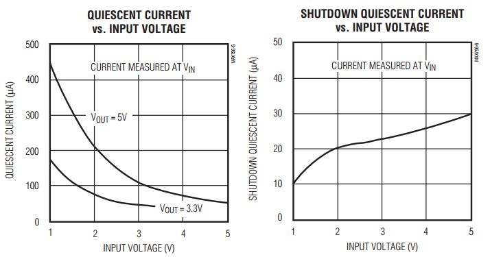
Here are its I_q profile:
 Suppose I'm using an Arduino nano (ATmega328) as the MCU and nRF24l01+ as the transmitter. I'm reading some sensor values via ADC and transferring the data over the RF link. So the system has a sampling frequency (suppose 100Hz).
If I want to save battery, the system should sleep most of the time and wake up and transfer the data 100 times a second. All Vccs should come from the boost converter. Now:
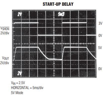
1- I should make MCU and nRF sleep but how about the step-up IC? Should it also be shutdown and waked up 100 times a second? I guess I should take the IC's start-up delay into account? Here is its profile:

Regarding this profile, I guess the IC wakes up in ~2ms... So the maximum sampling rate would be at best 500Hz?
2- What voltage would be on the OUT pin of MAX756 if it is shutdown? The same as Vin? or is it floating?
3- Is SHDN the same as Enable in different ICs?
4- If there is no way that the main MCU could control the SHDN pin, can I use like a 555 timer solution to control SHDN instead of an auxiliary tiny PIC MCU just for controlling the step-up IC? Because using a separate MCU just to control when an IC should shutdown seems to me rather an overdesign solution...Although if it is used in industry I have no problems then
Thank you very much
