5
\$\begingroup\$

I'm working on a mixed signal PCB that has some high-speed interfaces (HDMI, DDR, etc) I'm having some EMI issues on the HDMI that causes the product to fail radiated emission when the load is connected to the port via HDMI cable. While looking at the layout I noticed the CLK and data pairs each go through 3 vias between the connector and the uP.

  • Let's assume I have to use the number of vias I currently have due to space constraint. How important is via impedance to maintaining good signal integrity when dealing with high-speed interfaces?

  • What are typically the most important via parameters that can significantly affect signal integrity?

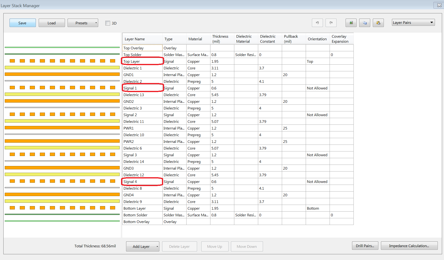
    enter image description here

enter image description here

Signal goes from inner-layer1 to TopLayer to inner-Layer4 to TopLayer

\$\endgroup\$
2
  • \$\begingroup\$ If you could show the relevant signals and returns in your layout someone may be able to spot something. \$\endgroup\$
    – Mike
    Commented Jul 13, 2017 at 12:32
  • \$\begingroup\$ @mike. I added a scope shot of one of the clock traces \$\endgroup\$ Commented Jul 14, 2017 at 19:36

2 Answers 2

1
\$\begingroup\$

Vias occur when you change layers. Changing layers requires the RETURN charges to also change layers, which provides lots of opportunities for radiation.

Place 1nF capacitors between the various planes, so the RETURN charges can hop between layers locally; you do not want charges to scatter everywhere, including PCB edges, in a desperate search for paths between layers.

\$\endgroup\$
2
  • \$\begingroup\$ Tightly coupled differential pairs are more robust to return discontinuities. Consider using as tight coupling as possible. Also, as analogsystemrf mentioned minimize return path discontinuities. If you reference the signals to a continuous ground plane drop ground vias near the signal vias. \$\endgroup\$
    – Mike
    Commented Jul 13, 2017 at 12:28
  • 1
    \$\begingroup\$ Read this about return discontinuities if you have more than one ground hottconsultants.com/techtips/pcb-stack-up-6.html \$\endgroup\$
    – DKNguyen
    Commented Feb 27, 2019 at 16:11
1
\$\begingroup\$

In general....

If you have to change layers, try to do it on either side of a reference plane. For example, L1 to L3 with L2 (GND) in the middle. Back-drilling the vias can help here by reducing stubs.

If you have to change GND planes stitch the planes with vias next to the transitions.

If the planes are different voltages, tie them with a cap at the transitions to provide the AC return path.

But really, try not to have vias at all on HDMI. Give them routing priority.

You may need to add CM filters on HDMI too. This gets tricky, as the filter influences the eye opening. But it may be what it takes for your system to pass.

With DDRx you have more leeway since you don’t have a cabling budget and the traces are shorter.

\$\endgroup\$

Your Answer

By clicking “Post Your Answer”, you agree to our terms of service and acknowledge you have read our privacy policy.

Not the answer you're looking for? Browse other questions tagged or ask your own question.