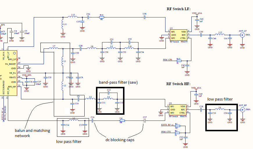
I am also currently trying to understand the TX path (on the LF side though) and I can tell that most of the time, the recommended schematics are full of unnecessary components (depending on what your application is), especially in RF.
About your analysis of the RX path, you got something wrong. C14, L5, C15 and C16 could be for filtering AS WELL AS matching the SX1276 RFI port (LNA). You can use a VNA to measure the impedance of that port (make sure to put your calibration plane @ C15) and then using these footprints (double L network, which is more than enough) to match the port to whatever reference impedance you need (usually 50ohms). Have a look at this AN:
www.semtech.com/images/datasheet/AN1200-16_SX1232_API_RF_ST.pdf
It explains the optimal way (different of mine) of matching the LNA (RF inputs) of the SX1200 family.
When designing such circuits, every single components have an effect on impedance matching. When some are chosen only to filter or DC bias/decouple the signal, others strictly have impedance matching purposes (I think C20 and L3 are some of those). C9, for example is used to block DC, but its value was also chosen accordingly to play a certain role in the TX matching network.
U4 (meant to be a SAW filter) and C17 are just shorts. There is no DC to be blocked here. C17 will be around 1nF which is a good RF short @ the operation frequencies of the chip. I would only put that capacitor since the 0 ohm resistor can have unwanted parasitic inductance (use thick film if you still want to put that 0 ohm for whatever reasons). Thats for RX.
TX is somehow a bit more complicated because it includes the Power Amplifiers Boost (PA_BOOST) options circuits. You can actually choose if you want to use that option or not. For this particular schematic, it seems the designer chose to use the PA_BOOST instead of the RFO_LF. And he used the standard PA for his HF band (RFO_HF).
Have a look at this AN:
http://www.semtech.com/images/datasheet/rf_design_guidelines_semtech.pdf
Page 12 reveals the purpose of most of the components. Then, the way they describe to match the port can be used if you have the right equipment. What you call the "Balun and Matching Network" circuit is not that at all. L1 and L2 are bias components that bring DC to the PA (PA_BOOST or RFO_XF). They are 100nH, so they basically block RF and let DC go through. C7 and C8 are large values that act as a RF RF ground. So, if some RF manage to get through L1 or L2, most of it goes down C7 and C8. They could also act as quick energy sources if the PA needs instant power. That said, you can see the PA_BOOST and the RFO_HF branches as two separate circuits. Nonetheless, you have to consider L1 and L2 when matching the RX/TX ports.
Here you'll find everything you need to know about the SX1276 and many reference design with Altium projects:
http://www.semtech.com/wireless-rf/rf-transceivers/sx1276/
Another note: The Pi-Networks next to the antenna connectors are only there to match the antennas to the RF switches which are usually 50 ohms. The commercially available antennas are rarely 50 ohms stock.
A+

