4
\$\begingroup\$

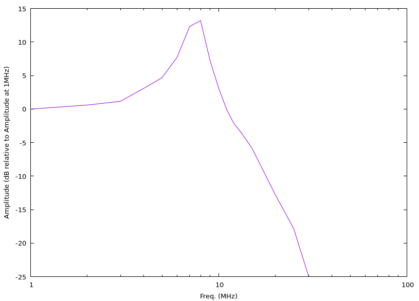
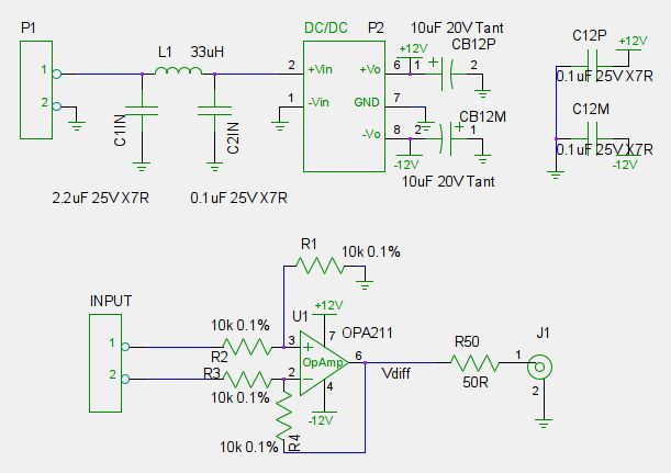
I'm using an OPA211 in differential mode with unity gain; no external compensation. I'm getting a puzzling ~10MHz bandwidth (specs indicate a bandwidth of 45MHz at G=1) with a peak at 8MHz (consistent with the horrible overshoot/ringing that I see when I feed a square wave input).

Here are the details of my design and my setup to measure the frequency response:

Schematic:

enter image description here

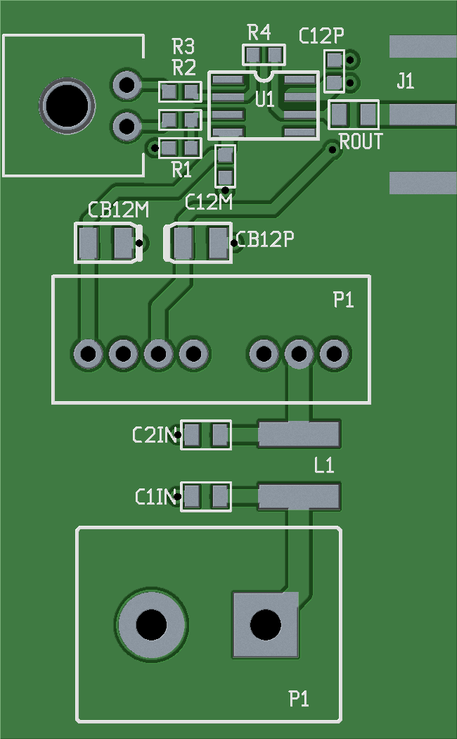
PCB:

enter image description here

And this is the frequency response that I get:

enter image description here

The ground plane is at the bottom layer, and the top layer has a copper fill that is connected to GND at the pins of the BNC edge connector (J1). This BNC connector (J1) is 50Ω; I connect it to a 50Ω BNC cable that goes to a 50Ω-terminated input capture device (a 180MSPS 16-bit Digitizer card on a PC --- the card itself specifies a 65MHz input bandwidth).

On the input side, however, there is no impedance matching --- to measure the frequency response, I use a signal generator with 50Ω BNC output, but I connected a cable that goes from BNC/coaxial to clips, and as you can see, the input goes to my board through a header type connector (more like a Molex-type, with locking housing).

BTW, when measuring the frequency response, I used a sine waveform with 100mV pk-to-pk to avoid issues with the slew rate (27 V/us as per the datasheet).

The ringing should not be surprising: it could be attributed to the op-amp getting closer and closer to instability when pushed to a low gain. But the low bandwidth is quite surprising --- precisely, at the lower gains I should expect higher bandwidth, right?

I also expect that parasitic capacitance or inductance (board, traces, ground plane, etc.) should not be an issue at such low frequencies (I would expect those to kick in at the hundreds of MHz range). For that matter, impedance matching (or lack of impedance control when ordering the PCB) should not play any role on the ringing at such low frequency, right?

Any ideas why such low bandwidth and why the peak at 8MHz?

\$\endgroup\$
1
  • \$\begingroup\$ With the right gain balance you could have 50/75 ohm (RF) or 600 ohm audio input with great performance. The key seems to be keeping the input resistors under 1 K in every case. \$\endgroup\$
    – user105652
    Commented Feb 8, 2018 at 4:50

4 Answers 4

6
\$\begingroup\$

Your resistors are too high value. Differential input capacitance of that op-amp is 8pF, which gives you a pole at 2MHz.

Parasitics from the ground plane are not helping either.

Try 1K resistors.

\$\endgroup\$
2
  • 1
    \$\begingroup\$ D'oh! Right, I had already looked at lowering those values, but didn't stop to think --- or do the math --- what the effect would be on this particular design! \$\endgroup\$
    – Cal-linux
    Commented Feb 7, 2018 at 19:35
  • \$\begingroup\$ Slightly better to use lower than 1k \$\endgroup\$
    – D.A.S.
    Commented Feb 7, 2018 at 22:59
5
\$\begingroup\$

The instability comes from stray positive feedback (p3) being more than the stray negative feedback (p2).

All it takes is 0.1pF difference at unit gain and you can get oscillation and your are almost there.

The resistors and the tracks form to make weak capacitors. Rf=500~750 is close to optimal for this part.

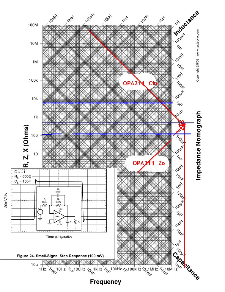
Layout is crucial in these designs. The ground plane should be removed from the area near the input pins to reduce stray capacitance. The Zo also rises to 50 Ohms @10MHz from lack of negative feedback gain which forms another LPF with 10k. @2MHz

Taking a closer look at the datasheet, Fig 24 shows the optimal response peaking with about 5% overshoot as they show is with 6.8pF of added neg. feedback and 680 Ohms for R instead of 10k. The 10pF load is intended to simulate a 10:1 probe may also affect this value.

This Op Amp is not ideal for a unity gain HF 50 Ohm buffer. enter image description here

The OPA211 Zout from the datasheet is equivalent to an impedance of 1 uH.

Conclusion:

You cannot always get full BW from unity gain at GBW product. This is a fact that Damn Fast Buffers are hard to perfect and this one is no exception. This IC has been surpassed by many others preceding it with 100x more bandwidth, using current feedback.

Even this one has 100MHz power bandwidth circa '75
my preference

If you want better results, give better specs. This one has a compromise in achieving very low noise and low supply current. What do you really need?

\$\endgroup\$
5
  • \$\begingroup\$ Couple of clarifications: (1) By "stray positive feedback (p3) being more than the stray negative feedback (p2)" you mean stray/parasitic capacitance from pin 6 to pin 3 is higher? (that seems sort of unavoidable, in that pin 3 is physically closer to pin 6 than pin 2). (2) Why does the open loop Zo matters? Once you use feedback, the output behaves as a nearly-Zo=0, but it doesn't matter, since it is the source of the wave; as for reflected waves coming back to the output, the 50-ohm Rout helps dissipate energy. Is my understanding flawed? \$\endgroup\$
    – Cal-linux
    Commented Feb 7, 2018 at 19:30
  • \$\begingroup\$ Zout=Zo/Av and when Av open loop =1 Zout=Zo and the stray pF matter when R feedback is too high. which is why they chose something < 1k.. If you learn how to compute ratios and intersect breakpoints, measure Q etc.etc on my log curve , is one way to look at it. \$\endgroup\$
    – D.A.S.
    Commented Feb 7, 2018 at 20:28
  • \$\begingroup\$ If you want a 50MHz linear gain, just say so and include all other specs \$\endgroup\$
    – D.A.S.
    Commented Feb 7, 2018 at 20:33
  • \$\begingroup\$ It's not so much a case of "I want 50MHz", it's more like "I need to see edges on squarewave differential signals, and I want those to be as sharp/fast and clean as possible".... I know that specs like "as ___ as possible" are dangerous --- one could always get to a $200M solution, which yes, is more ___ than the others! :-) I'm looking at alternatives such as the OPA847 (because it's pin compatible) and the THS4509... Now, you mentioned "current feedback" as a potentially better alternative. Could you comment on those vs. the couple of options I'm entertaining? \$\endgroup\$
    – Cal-linux
    Commented Feb 7, 2018 at 21:54
  • \$\begingroup\$ rise time 10~90% = 0.35/BW. How much BW you need depends precisely on rise time. Example 1ns rise time for 350MHz into 50 Ohms 10Vpp = 200mA/ns, 10V/ns is only 5% of 50MHz square wave to get 7th harmonic slightly attenuated .. like this? See my related answers electronics.stackexchange.com/questions/352304/… this will do 1.2Vpp with 1200V/us. Current is the problem G = +2, < 0.1 dB Peaking, Rf = 750 Ω 350MHz min 440 MHz typ 100R load OK with 50 source then coax then 50R term \$\endgroup\$
    – D.A.S.
    Commented Feb 7, 2018 at 23:04
3
\$\begingroup\$

Your not reading the fine details in the data sheet. The differential impedance is 20 K/8 pF. Figure 24 shows an inverter with a gain of -1 using 604 ohm resisters and a 5.6 pF feedback capacitor.

It is implied that a feedback capacitor is mandatory for stability, to overcome any parasitic positive feedback.

This ties in with Spehro Pefhany's answer, and that is to keep resistors at 1 K or lower, especially on the inputs. This is an RF amplifier, so treat it like one. That is has great audio parameters is just a sign of how much technology has advanced, but do not wire it up as an audio op-amp with 10 K resistor inputs, etc.

One drawing shows a gain of 10 with 1 K inputs and 10 K feedback. As a differential op-amp it would seem that 500 ohm inputs with a 10 K to ground and a 10 K feedback with a 4 to 6 pF feedback capacitor would max it out for a gain of 20 (26 dB) at a wide bandwidth.

The charts show a gain of 100 is possible but at severely reduced bandwidth. You can have a great audio amp, or a great RF amp, but not both at the same time.

\$\endgroup\$
3
  • \$\begingroup\$ Where does it say 5pF? Section 7.6 says 20k/8pF. Regarding Fig. 24 --- I figure the feedback capacitor is rather related to the capacitive load, no? The typical advice I've seen is to place the resistor in series as close as possible to the output to minimize the parasitic load capacitance. I guess I perhaps have a few pF (I'd guess considerably < 10pF, no?) parasitic from output to GND (when doing the layout I didn't pay attention to grounding and GND plane), so I guess I'll place a feedback cap anyway (at the very least it allows me to tune up with different capacitance values) \$\endgroup\$
    – Cal-linux
    Commented Feb 7, 2018 at 22:16
  • \$\begingroup\$ @Cal-linux. Voltage or power gain? 60 dB is a gain of 1000. \$\endgroup\$
    – user105652
    Commented Feb 7, 2018 at 22:51
  • \$\begingroup\$ @Cal-linux. I have corrected that 'bug' in the math. \$\endgroup\$
    – user105652
    Commented Feb 8, 2018 at 4:46
2
\$\begingroup\$

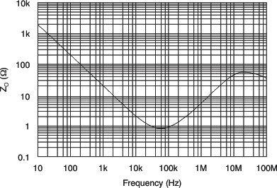
Any ideas why such low bandwidth and why the peak at 8MHz?
It's proabably due to the output impedance of the amplifier:

enter image description here

It looks like the output isn't matched to 50Ω at that frequency range (which proabably wouldn't be a big deal at 10MHz because transmission line effects aren't kicking in quite yet)

enter image description here

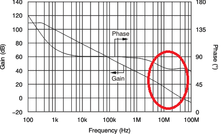
It also looks like they have two poles in the internal compensation of the amp to keep the pass band clean (indicated by the phase differences and the slight change of rolloff (in red))

I would try bandlimiting the amplifier and putting a pole in right before the 8MHz if that is acceptable

\$\endgroup\$

Your Answer

By clicking “Post Your Answer”, you agree to our terms of service and acknowledge you have read our privacy policy.

Not the answer you're looking for? Browse other questions tagged or ask your own question.