3
\$\begingroup\$

I am doing a simple project with MSP430FR6989, where I am converting an analog signal to a digital one, when it finishes conversion it will jump to an ISR and increment an integer.

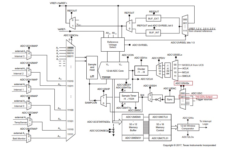
We can configure the ADC12_B (ADC module for the microcontroller) to start sampling and converting by setting ADC12SC bit from ADC12CTL0 register, or through various device-specific triggers.

enter image description here

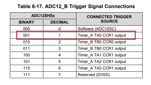
(User Guide pg 867/1021)

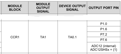
enter image description here

(Datasheet pg 91/183)

I am configuring my MSP430 to start converting using the TA0 CCR1 Output trigger (ADC12SHSx = 001)

With the information I have, I figured that if the CCIF bit of TA0CCTL1 register got set, it will trigger an ADC conversion, and when the conversion is finished and stored in the ADC buffer, an interrupt service routine will be triggered

I have written my code according to the information I have, build the project, and debug it, but during my debugging session my MSP430 never jumps to my ISR routine.

Can someone help me with that issue

This is a sample of the code I have written: inside the main() function:

int main (void)
{
    //code

    init_Timer ();
    //configures TA0 CCR1 to 50 ms

    init_ADC ();
    //ADC12SHSx = 001 (Trigger is TA0 CCR1)
    //ADC12IER0 = ADC12IE0; enables ADC12 Interrupt

    ADC12CTL0 = ADC12CTL0 | ADC12ENC; //enable Conversion

    _BIS_SR(GIE);//enable global interrupt

    //rest of code
}

inside the ISR function

#pragma vector = ADC12_VECTOR
__interrupt void ADC12_ISR (void)
{
    static int x = 0;
    ++x;
}

EDIT_0

inside the init_ADC () function

void init_ADC (void)
{
    ADC12CTL0 = ADC12ON | ADC12SHT0_2;
    //ADC ON, 16 ADC12CLK

    ADC12CTL1 = ADC12SHS_1 | ADC12SHP | ADC12SSEL_1;
    //TA0 CCR1 Output, SAMPCON from Sample Timer, ACLK

    ADC12CTL2 = ADC12RES__12BIT;//12 bit resolution

    ADC12MCTL0 = ADC12INCH_10;//A10 P9.2

    ADC12IER0 = ADC12IE0;//enable MEM0 interrupt (if it's value changed)
    ADC12IFGR0 = ADC12IFGR0 & (~ADC12IFG0);
}

Inside init_Timer () function

void init_Timer (void)
{
    TA0CTL = MC__UP | TASSEL__ACLK;//counts to TA0CCR0, and source from ACLK

    TA0CCR0 = 1667;//50 ms count = 50/.03 (Tperiod of ACLK = .03)
    TA0CCR1 = 1667;// 50 ms
}

END of EDIT_0

\$\endgroup\$
4
  • \$\begingroup\$ Could you provide Timer and ADC initialisation code, please? \$\endgroup\$ Commented Oct 24, 2018 at 10:57
  • \$\begingroup\$ @GVelascoh Sure I will do that right now in the edit (EDIT_0) \$\endgroup\$ Commented Oct 24, 2018 at 11:01
  • \$\begingroup\$ Personally, I like doing things the other way. Use a timer interrupt to service the data, when you pretty much know it's ready, and then trigger the read, \$\endgroup\$ Commented Oct 24, 2018 at 12:02
  • \$\begingroup\$ I am learning about the ADC12_B module, so I would like to explore as many features it has. Even though, eventually I would like to put my uC in a Low Power Mode, and if I have a Timer ISR that triggers a conversion which goes to an ADC ISR, these 2 instances would wake the uC from it's sleep, if I only use one ADC ISR and let it get triggered by the "TA0 CCR1 Output" I feel I would save some power consumption, as it will wake up once for every cycle \$\endgroup\$ Commented Oct 24, 2018 at 14:05

2 Answers 2

1
\$\begingroup\$

Table 6-12 in the datasheet also shows how the ADC trigger input is connected to the timer:

MSP430FR6989 TA0 output

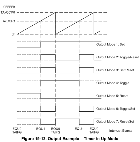
And this makes clear that the "timer output" is the same signal that would be output to a GPIO pin. In other words, this has nothing to do with the interrupt itself, but you have to configure the output mode to generate a rising edge at the desired time. The default output mode (0) never changes the output; you want something like "Toggle" or "Set/Reset", depending on the frequency:

MSP430 timer output modes

\$\endgroup\$
4
  • \$\begingroup\$ The ADC Interrupt got nothing to do with the start/triggering of the conversion, the interrupt is for when the value at ADC12MEM0 changes and ISR will occur. This is what I figured, if it is not the CCIFG of TA0CCTL1 then, it is the output from TA0.1, I changed the output mode of the CCR1 module, to output mode 4: Toggle, where I set it to toggle every 50 ms. This is what confuses me, in table 6-12 it mentions that in order to make a signal connection to ADC12, the Device Input Signal, and the Module Input Signal to be DVss and GND, or DVcc and Vcc respectively \$\endgroup\$ Commented Oct 24, 2018 at 16:01
  • \$\begingroup\$ The timer's inputs and outputs are completely independent, and configured separately. \$\endgroup\$
    – CL.
    Commented Oct 24, 2018 at 17:28
  • \$\begingroup\$ Sorry, I don't quite understand, how can I make the CCR1 module triggers the ADC12. I went to the User Guide page ... Figure 25-1, there you will see CCRx module with inputs from CCIA, CCIB, GND, Vcc, all configured via the CCIS bits from the TA0CCTL1 register, I changed my code accordingly (CCIS = GND, and CCIS = Vcc), and still there is no change \$\endgroup\$ Commented Oct 24, 2018 at 18:44
  • \$\begingroup\$ Again: the timer inputs do not matter. You are not using capture mode but compare mode. \$\endgroup\$
    – CL.
    Commented Oct 24, 2018 at 20:14
0
\$\begingroup\$

You could try to enable the timer interrupt and check that CCR1IF is going high and that SAMPCON is set afterwards. Also, you can check ADC registers as well, to determine its status, e.g. ADCBUSY bit. It is a good idea to use switch-case on ADC12IV and enable error-related interrupts to debug.

Please let me know how it is going.

\$\endgroup\$
5
  • \$\begingroup\$ I am learning about ADC12_B module, so I want to know how to trigger it using "TA0 CCR1 Output". My original ISR was more complex, and had a switch statement for ADC12IV reigister (still faced the same problem), then to check what is wrong with my ADC, I did the simpler code that I posted here. I tried debugging, by setting the CCIF bit from TA0CCTL1 register, that didn't do anything, I will try again, and update you. \$\endgroup\$ Commented Oct 24, 2018 at 11:56
  • \$\begingroup\$ Hi, I just check this line ADC12CTL0 = ADC12CTL0 | ADC12ENC; //enable Conversion. You are assigning to the register ADC12CTL0 its address value, but I think you want just to set the ADC12ENC bit without affecting its current value, so you should use ADC12CTL0 |= ADC12ENC; instead \$\endgroup\$ Commented Oct 24, 2018 at 14:31
  • \$\begingroup\$ No, I don't think this is the case, ADC12ENC is a macro defined in msp430fr6989.h library and I am doing a bitwise OR operation between ADC12CTL0 register, and ADC12ENC so that the ADC12ENC bit in ADC12CTL0 register will be set without changing the values of the original bits in the register \$\endgroup\$ Commented Oct 24, 2018 at 16:05
  • \$\begingroup\$ I understand what you want to do. Indeed ADC12ENC is a macro and is ok to use it to set the correspondent bit, but at that point what is the content of ADC12CTL0? \$\endgroup\$ Commented Oct 24, 2018 at 16:16
  • \$\begingroup\$ Also, you could try using mode 7 instead of mode 4, and set a small value in TA0CCR1, because you need to generate both edges (to sample and convert). \$\endgroup\$ Commented Oct 24, 2018 at 16:33

Your Answer

By clicking “Post Your Answer”, you agree to our terms of service and acknowledge you have read our privacy policy.

Not the answer you're looking for? Browse other questions tagged or ask your own question.