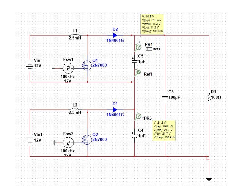
I need to make a simulation of multiple boost converter design for different load ratios. I have designed 2 boost converter both of them have same duty cycle and same L and C values. Voltage input is 12V and with 50% duty cycle I expect to see 24V output from each of them. If I connect them in series I should get arround 48V total output, but for some reason, the top boost converter voltage is pulled down and not giving 24V. Can someone notice my mistake ot give me some tips? thank you
2 Answers
If the source of Q1 is at 24 volts and the gate signal (Fsw1) rises from 0 volts to 12 volts then the top boost converter will never activate its MOSFET (Q1) try connecting Fsw1 between source and gate of Q1.
You might also stringly consider swapping the diodes (1N4001 types) with something that can handle switching voltages in the hundreds of kHz.
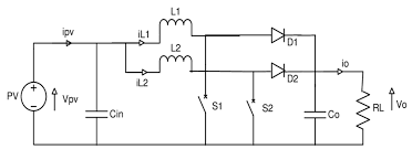
 https://www.researchgate.net/figure/Interleaved-boost-converter_fig2_324822323
Your circuit reminds me of an interleaved boost converter.it utilizes two inductors and two swicthes thus reducing the overall stress on the inductors because two inductors are sharing the current equally.Btw connecting boost converters in series is not really a good idea.because there is a ohmic connection to output and input,but its still possible to connect converters in series.click the link below for more understanding on this topic
https://electronics.stackexchange.com/a/91613/281776
If the inductor is isolated type for example flyback converter its possible to connect them in series.if you want to increase the voltage you can increase the duty cycle or increase the number of turns.
Here is a nother way getting higher voltage
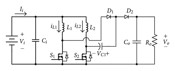
 https://www.hindawi.com/journals/tswj/2012/896508/
This circuit is a interleaved high voltage boost converter it works like a voltage doubler stage and it has very low voltage ripple thus increasing the efficiency
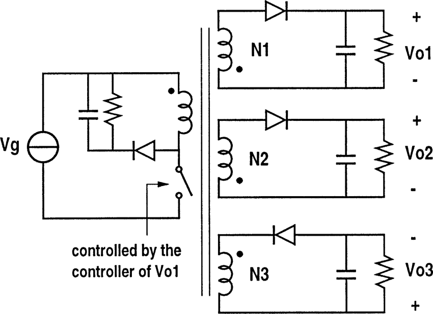
 https://www.researchgate.net/figure/Isolated-multiple-output-converters-a-Forward-converter-b-Flyback-converter_fig1_2982127
This is the trusty old flyback converter
This circuit is more flexible because you can use different secondary winding ratio and configuration like series and parallel and its galvanically isolated.
Btw as @Andy suggested use a fast shottky diode
That can handle the voltage and current,hope this helps.

