2
\$\begingroup\$

EDIT: I edited the question as it was my misunderstanding to think that the transistor was not getting into saturation.

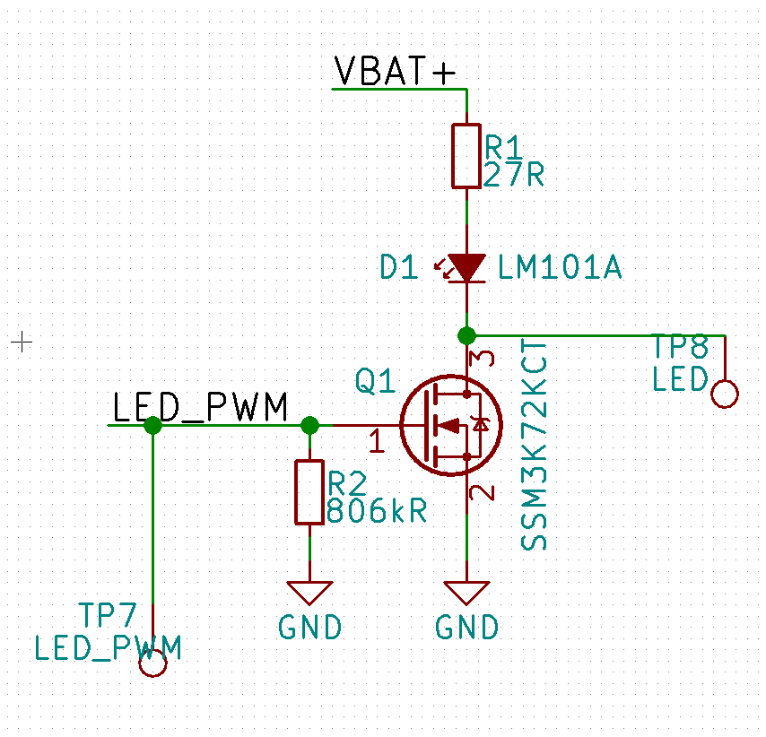
I'm driving an LED with a microcontroller through a transistor with a PWM signal.

enter image description here

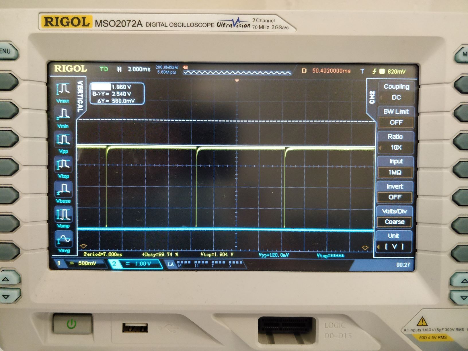
When the gate is grounded, no current flows, as expected. As soon as I start to drive the transistor (1% duty cycle), I get a voltage drop in TP8 of ~2V, with a 1% of the cycle at 0V. This turns the LED on at quite a high level of brightness, way more than 1% DC from the battery voltage would suggest.

enter image description here

As the duty cycle increases, the semiperiod at 0V at TP8 increases (as expected). The result is that VLED is something like (b), instead of seeing something like (a).

$$(a) Duty Cycle * 3.3V \\ (b) DC_{value} + ((3.3-DC_{value}) * Duty Cycle)$$

My PWM frequency is rather low, as I'm using a low frequency clock to generate it, so it's only 128Hz, and I have an 8 bit resolution. The positive rail for the LED is the battery voltage, so it will vary from 4.2V to 3.XV. The MPN of the LED and the transistor are in the schematic (Transistor datasheet, LED Datasheet). The threshold voltage of the transistor is 2.1 in the worst case, so I can't see why is not fully switching.

Can somebody shed some light?

edit: I am expecting the voltage at TP8 to go to 3.3V, but it's 1.6V. If the pin is technically floating, why can't I measure 3.3V at TP8?

\$\endgroup\$
5
  • 3
    \$\begingroup\$ Reduce R2 to 1k \$\endgroup\$
    – D.A.S.
    Commented Mar 15, 2019 at 17:04
  • 4
    \$\begingroup\$ @SunnyskyguyEE75 Can you explain how reducing the value of R2 will decrease Vds? Comments like this with no explanation aren't very helpful in general. I would expect that a low value for R2 would cause the high-time voltage of the PWM signal to decrease, making matters worse instead of better. But I would be happy to be educated. \$\endgroup\$ Commented Mar 15, 2019 at 17:35
  • \$\begingroup\$ Although 128 Hz is very slow the ratio of Rg to Ron ought to be < 5k and for higher speeds < 1k and at max speed <100 . This is because of the Ciss*RdsOn constant / I thought at first it said 128kHz so it is not a solution here. but just a general rule of thumb. Meanwhile 3.6V logic impedance is < 50 Ohms so 1K does not drop the drive level much... here with a 50 Ohm drive, it won't matter but 806k seems to be a peculiar choice of values. trying to save a mV when he needs at least an extra volt on Vgs \$\endgroup\$
    – D.A.S.
    Commented Mar 15, 2019 at 17:39
  • \$\begingroup\$ I can understand wanting to reduce series resistance to the gate, but as you said the output impedance of the logic is much lower than even 1 kilohm. So I guess we are agreed that it really doesn't matter whether R2 is 1k or 100k or 800k, as long as the gate is driven by a low impedance logic output. \$\endgroup\$ Commented Mar 15, 2019 at 18:03
  • \$\begingroup\$ Thanks for your replies. The reason why I pointed the PWM freq was to show that it was not a matter of the transistor not switching fast enough. About the R2 (Rg), I'm afraid that I inherited the design and the previous engineer didn't record any design intents anywhere, so I'm as puzzled as you are about the choice of an 806k. About GPIO output impedance, well, you could expect it to be relatively low: the two data points given by the datasheet are 220Ω when the drive strength is set to "low" and 33Ω when is set to "high" at 3.3V and 8mA. \$\endgroup\$ Commented Mar 19, 2019 at 11:47

2 Answers 2

1
\$\begingroup\$

When the voltage at the gate of the transistor is 3.3V, the transistor goes into saturation, and the voltage at TP8 is close to 0V.

When the voltage at the gate of the transistor is 0V, the transistor goes into cutoff, and TP8 is left floating. I was expecting it to read 3.3V, given that one pin of it is connected 3.3V via the current-limiting resistor, but that's not the case as there's a diode in the between, isolating TP8 from 3V3.

\$\endgroup\$
0
\$\begingroup\$

So many people confuse Vth or Vt or Vgs(th) with the required gate voltage to guarantee RdsOn.

If you read the specs carefully the conditions for Vth are VDS = VGS, ID = 250 µA

This means a 2.1V Vds/ 250µA = 8.4Kohm resistor the so-called threshold of conduction.

Normally you need at least 1.5x Vt max and typically 2x to 3x Vt but here they only guaranteed RdsOn at Vgs=4.5 (4.5/1.6Vtnom = ~3x Vt)

So you are seeing the effects of insufficient gate drive to achieve 1 Ohm RdsOn.

This means if low battery is 3.0V you need a Vgs(th)=1.1V max

e.g.DMG1012UW-7

Other points to consider

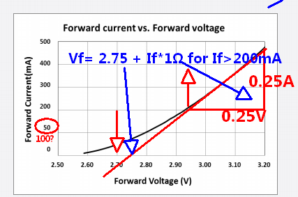
Also if you wish to regulate current, there are better ways to keep it constant, but you may compute \$I_f\$ as battery reduces from 3.7 to 3.0V using KVL with this formula. Note the curves are typical and not guaranteed so they have a tolerance of often +25%/-12% even on the best Samsung parts, where others might be +50%/-15% (ballpark)

enter image description here

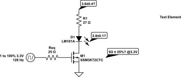
If=V/R= (Vbat-2.7V)/(RdsOn+Rled+Rs) ( for If>200mA) If you choose my suggested part, RdsOn=0.5 Ohm @ 3V(Vgs)

\$R_s=\dfrac{(V_{bat}-2.7)}{I_f}-R_{dsOn}-R_{led}\$ e.g.

So if you wanted 200mA at 3.8V, Rs=1.1/0.2 -0.5-1= @ 1/4W (not 27Ω) but at 3.0V If<0.3/5.5=55mA why "If<" because Rled is now ~2Ω so If~0.3<6.5= 46mA . A 1W LED needs at least 6cm² surface area heatsink.

schematic

simulate this circuit – Schematic created using CircuitLab

\$\endgroup\$
8
  • \$\begingroup\$ Hi, sorry for my late reply. This was moved to the low priority queue :D Thanks for the suggested part: sadly, we are very space-constrained, so we will have to keep the current form factor (but will use your suggestion when sourcing an alternative). In any case, you reply seems to be oriented to achieving full conduction, but my problem is the contrary. When I apply 0V, I get a drop of 1.6V at the transistor gate. I would expect it to be off, and get 3.3V. I'll edit my question to make it clearer \$\endgroup\$ Commented Apr 1, 2019 at 13:22
  • \$\begingroup\$ You mean when you apply Vgs=0V you get Vds=1.6V at drain, which is normal with even 1uA of leakage. Just add a Pullup R to supply the leakage current. \$\endgroup\$
    – D.A.S.
    Commented Apr 1, 2019 at 13:28
  • \$\begingroup\$ You will get very poor current regulation with Vbat 3 to 4V with Vled=2.8 +0.2/-0.1 \$\endgroup\$
    – D.A.S.
    Commented Apr 1, 2019 at 13:43
  • \$\begingroup\$ Hi, Thanks again for your help, I am very grateful. I think that I misunderstood the issue. My problem is that I was expecting to measure 3.3V at TP8 when the transistor gate was low and the transistor was in cut off. The problem is that there's a diode between 3.3V and TP8, so TP8 won't see the 3.3V. I think the transistor works perfectly, it's me that was expecting something else. \$\endgroup\$ Commented Apr 1, 2019 at 14:20
  • \$\begingroup\$ What tolerance do you expect on output Ipk with tolerances on Vbat and Vgs ? It seems quite wide. You could use PD feedback to regulate it. \$\endgroup\$
    – D.A.S.
    Commented Apr 1, 2019 at 14:25

Your Answer

By clicking “Post Your Answer”, you agree to our terms of service and acknowledge you have read our privacy policy.

Not the answer you're looking for? Browse other questions tagged or ask your own question.