0
\$\begingroup\$

I have two versions of the input signal:

  • 5V inactive level, 3.2V active;
  • 5V inactive level, 0V active level.

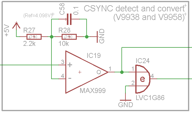
Thinking on making universal circuit to support both signals, I decided to use comparator, having threshold voltage at about 4V. Here's the circuit:

enter image description here

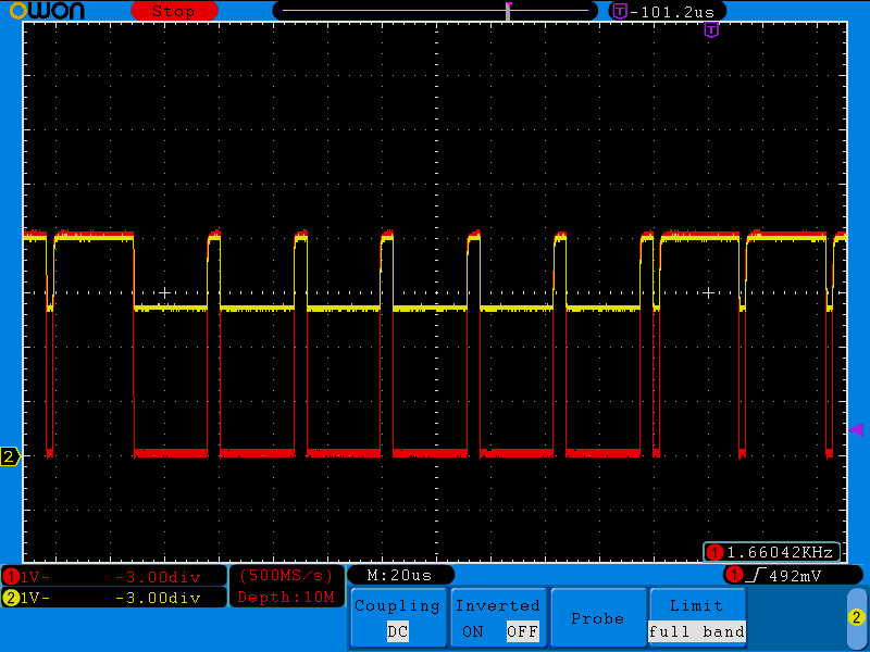
I built a prototype, and it shows unexpected (for me) behavior:

enter image description here

Red is voltage on positive input pin, yellow is on negative. Capacitor C58 was removed.

Searching through internet I found this question. It is about operational amplifier, and not about comparator. But I took a closer look into the datasheet, and found the following:

Differential Input Clamp Voltage --- VCC = 5.5V, VIN- = 0V, IIN+ = 100µA --- 2.1 V

Is it the information I should be looking at? Does it mean that voltage between + and - inputs must be not larger than 2.1 V, otherwise there will be current path between the inputs? Is it naive to assume that if I have comparator powered from 5V, that it must be able to properly handle differential voltages on the whole power scale? And why datasheet does not state that there's such a limitation in its headline?

Update:

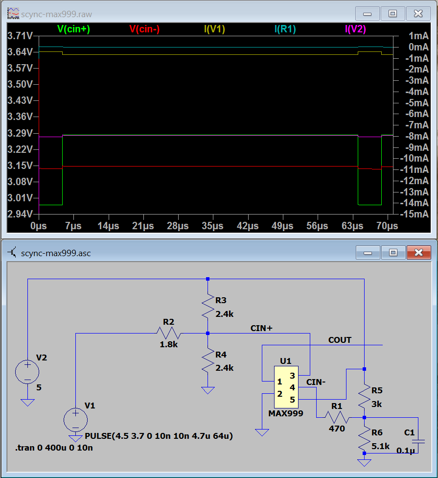
After considering answers below I decided to stick with MAX999 so far, and designed the following circuit:

enter image description here

I still think it is an overkill, but at least it is expected to work properly:

  • supply current is about 8 mA. In my previous simulations MAX999 model was failing when IN+ was approaching IN- starting consuming about 60 mA, most probably because of issues in definition of the input stage circuitry.
  • digital input was resized and re-leveled (green), with reference voltage placed into the exact center of the worst case for the input signal;
  • circuit draws less than 1 mA from the positive input, and almost nothing through the negative input;
  • power on current is much less than 10 mA, limited by the 470 Ohm resistor;
  • differential voltage does never go out of 2.1 V range.
\$\endgroup\$

2 Answers 2

1
\$\begingroup\$

IIN+ = 100μA 2.1V means you may limit current the source voltage with a series R 2.1V/100 μA =21k is the threshold of conductance of the clamp.

Current into Input Pins .....................................................±20mA

Then consider driver Vol/Iol limits and (Vol(=0 @ 50 Ohms)) Thus divider divider is 4V (=Veq) / 1.8k (=Req) = 2.22 mA So you are OK. But with cap you need to add 330R ~1k in series = Rs on input.

Your driver Spec = TBD

\$\endgroup\$
3
  • \$\begingroup\$ I see. Do you think I may need to consider different comparator for this input signal - decreasing number of components, supply current and complexity? E.g. MAX9010 having 250 kOhm of differential input resistance, and not having clamp diodes? \$\endgroup\$
    – Anonymous
    Commented Aug 1, 2019 at 20:53
  • \$\begingroup\$ I don't see any reason since you do not have any specs or measurable design goals. \$\endgroup\$
    – D.A.S.
    Commented Aug 1, 2019 at 23:22
  • \$\begingroup\$ Special thanks for suggestion on series resistor because of capacitor. \$\endgroup\$
    – Anonymous
    Commented Aug 2, 2019 at 14:33
1
\$\begingroup\$

If you look at the MAX999 data sheet again you will see this on page 2: -

Differential Input Impedance @ VCC = 5V 8 kΩ

And this is more likely giving you the effect you see although the clamping voltage at 100 uA is also contributing.

\$\endgroup\$
5
  • \$\begingroup\$ Thank you. I am almost convinced that I have simply chosen wrong comparator device. To minimize number of components it must withstand full scale voltage (as described by the input signal definition). Supply is 5V. Small logic (one piece). 10 ns would be ok. What comparator (family) would you recommend for the task? I am not looking for the "personal opinion", I am lookign for guidance as comparator devices are abundant but I prefer not to look through all the possible datasheets. \$\endgroup\$
    – Anonymous
    Commented Aug 2, 2019 at 9:00
  • \$\begingroup\$ Wrong device? Maybe not - what actual problem is the disturbance on -Vin actually causing? If you made R27 220R and R28 1kohm would that be a problem? And, remember you have removed C58. The MAX999 is a really good device and maybe you are seeing something that is basically "as per the data sheet" but isn't an issue. \$\endgroup\$
    – Andy aka
    Commented Aug 2, 2019 at 9:22
  • \$\begingroup\$ Absolutely, it is per datasheet. It can not handle 5V differential voltage per design, requiring constructing resistor networks to support this environment. And it is really good device, I agree. What I actually said is that there may be better device for this application? Probably the cause for my question is that I do not fully get Sunnyskyguy's answer... I think he suggests putting 21k resistor in series with the input, but I guess there must be solutions (and related chips) when I need not doing it. --- And I think that current being drawn through the negative input is a design issue... \$\endgroup\$
    – Anonymous
    Commented Aug 2, 2019 at 9:36
  • 1
    \$\begingroup\$ If you look at page 9 it shows the equivalent of the input. This means 2.1 volts across the 3 diodes and, if 5 volts is applied differentially, the resultant voltage across 2 x 200 ohms is 2.9 volts hence, current is 7.25 mA (absolute max limit is 20 mA so no worries here). However, ff this upsets your input driving stage then you should look for an alternative. There were some fast ones by LT (now owned by ADI). The LT1719 springs to mind but it may be no better than the 999. \$\endgroup\$
    – Andy aka
    Commented Aug 2, 2019 at 10:05
  • \$\begingroup\$ @Anonymous are we done with this Q and A now? \$\endgroup\$
    – Andy aka
    Commented Jan 27, 2021 at 14:12

Your Answer

By clicking “Post Your Answer”, you agree to our terms of service and acknowledge you have read our privacy policy.

Not the answer you're looking for? Browse other questions tagged or ask your own question.