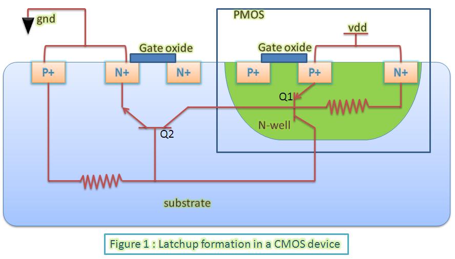
Actually, the Schottky clamping diodes and the VDD + 0.3V are both present for the same root cause and that is SCR Latch-up. The design of all CMOS ICs actually creates a pair of BJT transistors intrinsically. It simply results from out the p-type and n-type silicon substrates are laid out. This picture from VLSI Universe shows it well:
https://1.bp.blogspot.com/-yUiobLvxMrg/UTvnjjzaXZI/AAAAAAAAABc/lRFG5-yqD3E/s1600/latchup.JPG
You get two intrinsic BJT transistors, Q2, and NPN, and Q1, a PNP. Note, they share the one N-well and one P-well, but this particular arrangement forms something called a Silicon Controlled Rectifier (SCR). This is not desired in anyways, but an unfortunate side-effect of this arragement. It is not a problem if certain rules are followed.
A typical SCR has three terminals, Anode, Cathode, and Gate. In general, it is forward-biased for some device that must be controlled with a positive voltage at the Anode with respect to the Cathode, however, the SCR will block any current unless the Gate is activated. To activate the Gate, it must rise across a threshold which, in this design, will be the Anode voltage. One the latch is activated, it will stay on even if the Gate drops. It will stay on until the Anode voltage drop to near zero current. For the CMOS IC, the Cathode is akin to the chips GND, the Anode is the VDD rail, and the Gates are the I/O Pins. This is the crux, if any I/O pin rises much above VDD, it will enable the latch and create a short between VDD and GND causing a very large amount of current and that current will keep the latch going burning up the IC.
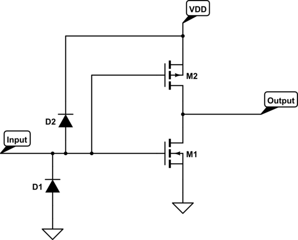
To help protect against this for small transient spikes, Shottky diodes are added to the I/O lines to clamp the input to GND - 0.3V and VDD + 0.3V inside the safe zone. These diodes can only take a small amount of current and external clamping can still be required for more rugged designed.
For more info, EEVblog did a nice tutorial on this: EEVblog #16 - CMOS SCR Latchup Tutorial


