0
\$\begingroup\$

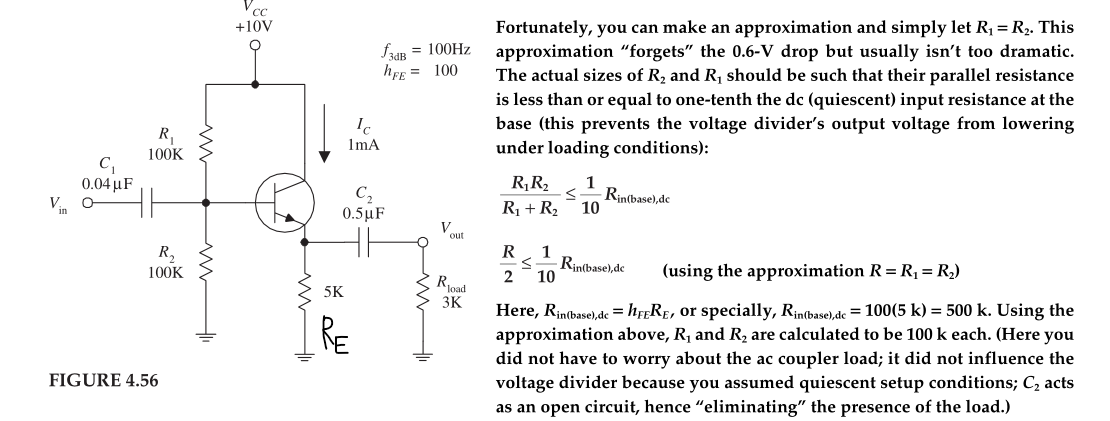
I'm studying the emitter-follower configuration for bjt on the book "Practical Electronics for Inventors". On pag 439 there is an example related to the design of this system. In this problem it knows the parameters Rload, Vcc, hfe and f3db, and the target is to find the other parameters:

  1. choose the value of Ic = 1mA;
  2. Find the resistance Re = (0.5*Vcc)/Ic;
  3. Find the ratio of R1/R2 such that Ve = Vb-0.6V;

Than it says that R1//R2 <= 0.1 Rin(base),dc because this prevents the voltage divider's output from lowering under loading conditions. I don't understand this statement.

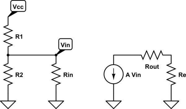
My first question is: why R1 and R2 are in parallel? If you apply the simplified model (I show after) to find the quiescent operating point R2//Rin not R1//R2. Am I wrong? Con you explain the meaning of this statement?

Thanks

enter image description here

Equivalent model

schematic

simulate this circuit – Schematic created using CircuitLab

\$\endgroup\$

1 Answer 1

1
\$\begingroup\$

this prevents the voltage divider's output from lowering under loading conditions

This is correct.

R1 and R2 act as biasing resistors -- they're meant to generate a DC voltage that biases the transistor in a suitable operating point. The signal itself is injected via C1.

You could think of the four currents going into or out of this node: those from/to C1, R1, R2 and the BJT's base terminal. If we took out C1, then we'll have a certain voltage at the BJT's base terminal, biasing it at a certain operating point.

When you add C1 back in, it's going to source/sink a certain current from that equilibrium point, and therefore change the voltage on that node (by sourcing/sinking extra current from the other nodes; after all, Kirchhoff's current law must still hold.) If the current is significant in comparison to the equilibrium, then it's going to disturb the operation point and exacerbate the non-linearities of the BJT.

Therefore, making sure the bias resistors' current is significantly higher (10x in this case) than the input current is an attempt to bound the errors due to the BJT's non-linearities.

why R1 and R2 are in parallel?

Forgetting about the input voltage for a moment, transform the circuit composed of Vcc, R1 and R2 into its Thevenin equivalent model. What do you get?

If you apply the simplified model (I show after) to find the quiescent operating point R2//Rin not R1//R2. Am I wrong?

You are wrong. Nobody models BJT circuits this way. Google for (or look up in your book) "hybrid-pi model" or "T model".

\$\endgroup\$
4
  • \$\begingroup\$ I think, the above explanation is NOT CORRECT. The original text speaks about the DC input resistance at the base. That means: The current through the divider chain (100k/100k) should be at least 10 times the DC input current at the base. Such DC considerations have NOTHING to do with the coupling capacitor. For IC=1mA and assuming B=100 we have IB=10µA.This is compared with the current 10V/200k=0.1mA=100µA (which is exactly 10*IB). Note, the base divider is loaded by the base input (not by the coupling capacitor) \$\endgroup\$
    – LvW
    Commented Mar 19, 2020 at 14:24
  • \$\begingroup\$ Alternativ calculation: DC input resistance: Rindc=Vbase/Ib=(IE*RE+0.6)/10mA=5.6/10µA=560kOhms. In the text, Vbe=0.6V was neglected, resulting in 500k, which leads to the requirement 100k||100k=50k=0.1*Rindc (the parallel combination results from the Thevenin equivalent) \$\endgroup\$
    – LvW
    Commented Mar 19, 2020 at 14:39
  • \$\begingroup\$ Thank you for the answer,I think that the @swineone is corrent. If you consider my last circuit and substitute R1 and R2 with the parallel R1//R2, you'll get that the voltage VB = (Rin*Vth)/((R1//R2)+Rin) if (R1//R2)>>Rin, the changes in Rin will not affect the Vb voltage. \$\endgroup\$
    – Ugo Mela
    Commented Mar 19, 2020 at 15:17
  • \$\begingroup\$ No, @swineone is not correct - as far as his considerations regarding the coupling capacitor are concerned. More than that, he has mentioned "non-linearities" - which are not the reason for the mentioned rule of thumb (factor 10). The actual background is the following: The base voltage created by the voltage divider should be as "stiff" as possible because of the negative feedback effect caused by the emitter resistor RE (which works best for a fixed base voltage). \$\endgroup\$
    – LvW
    Commented Mar 19, 2020 at 17:01

Your Answer

By clicking “Post Your Answer”, you agree to our terms of service and acknowledge you have read our privacy policy.

Not the answer you're looking for? Browse other questions tagged or ask your own question.