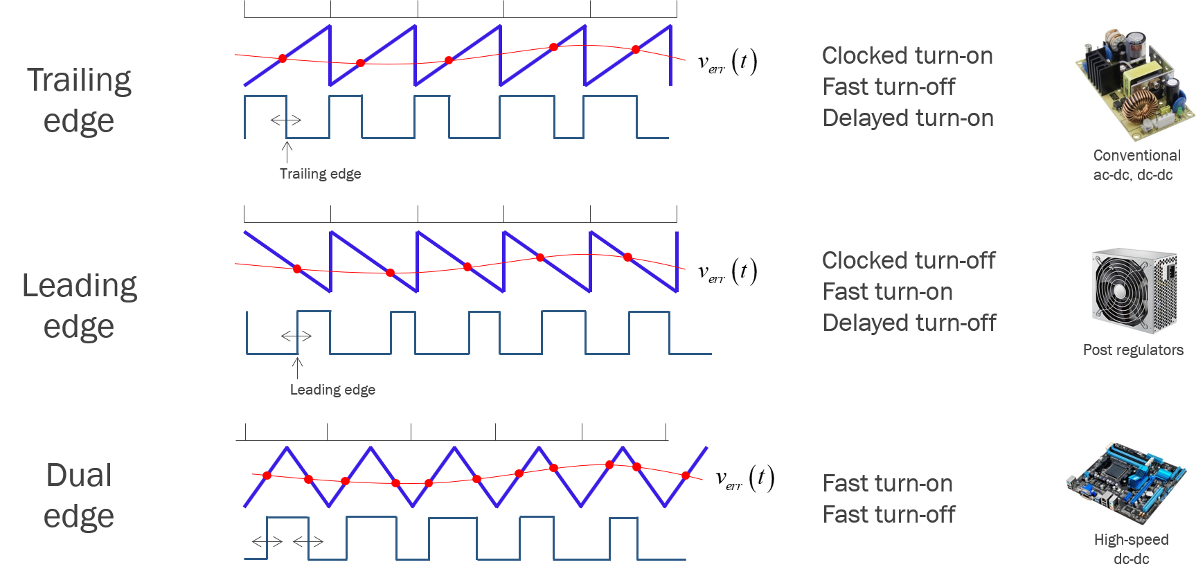
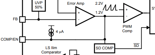
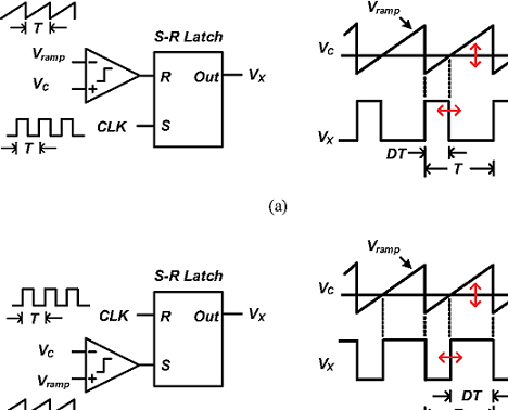
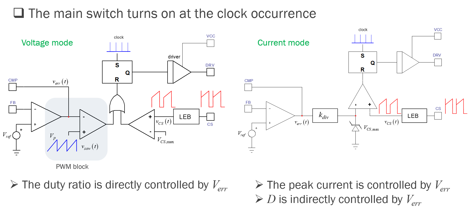
There are various types of modulation schemes whose choice depends on the end application. The most common type is the trailing edge modulator. In this type, the on-time is initiated by the clock while the loop sets the event at which the switch turns off. The below circuit shows a typical industrial implementation in an integrated circuit for both voltage- and current-mode control:

This is an excerpt of the seminar I taught at APEC in 2019.
The second type is called leading-edge modulation. In this approach, the clock sets the turn-off time while the loop set the events at which the turn-on occurs within a switching cycle. This technique was popular in so-called magnetic amplifiers, commonly known as mag-amps and implemented in the PC silver boxes (power supplies) for multi-output solutions. More more modern solutions known as mag-amps killers were released and also based on leading-edge modulation. They are described page 866 in the book I published in 2014.
Finally, the dual-edge modulation is implemented in high-speed dc-dc converters used in motherboards or graphic cards where reaction speed is key: in the trailing-edge approach, when the switch has turned off, you have to wait for the end of the cycle so that the next clock initiates a new turn-on. Same with the leading-edge scheme where you can't turn off before the clock occurs. As you can see, reaction speed in case of under- or over-shoot is at stake and can affect performance in highly-demanding applications where the over- and under-shoots must really be minimized. The below picture gives an overview of these techniques:
