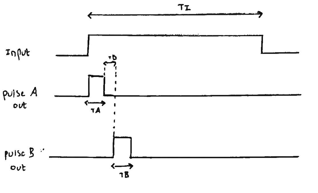
I have designed a small circuit to perform the following functional purpose as illustrated below. The circuit takes a PWM signal as input from a microcontroller and outputs two smaller pulses (ideally between 0.5\$\mu\$s and 10\$\mu\$s) - In practice I can achieve a minimum of 1\$\mu\$s. The pulse widths and delay between the two pulses are adjustable via potentiometers such that TA,TD and TB are adjustable independently.
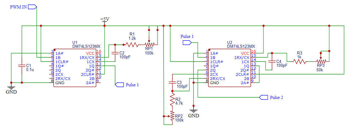
I originally designed this circuit around some 555 timers however quickly realised that this choice of IC was a bad one because the minimum pulse width I could get was around 7\$\mu\$s. I've now designed the circuit using the DM74LS123 as shown below:
The circuit above is based on the delay circuit in this application note (page 14). It uses two ICs with only the first half being used on the first IC.
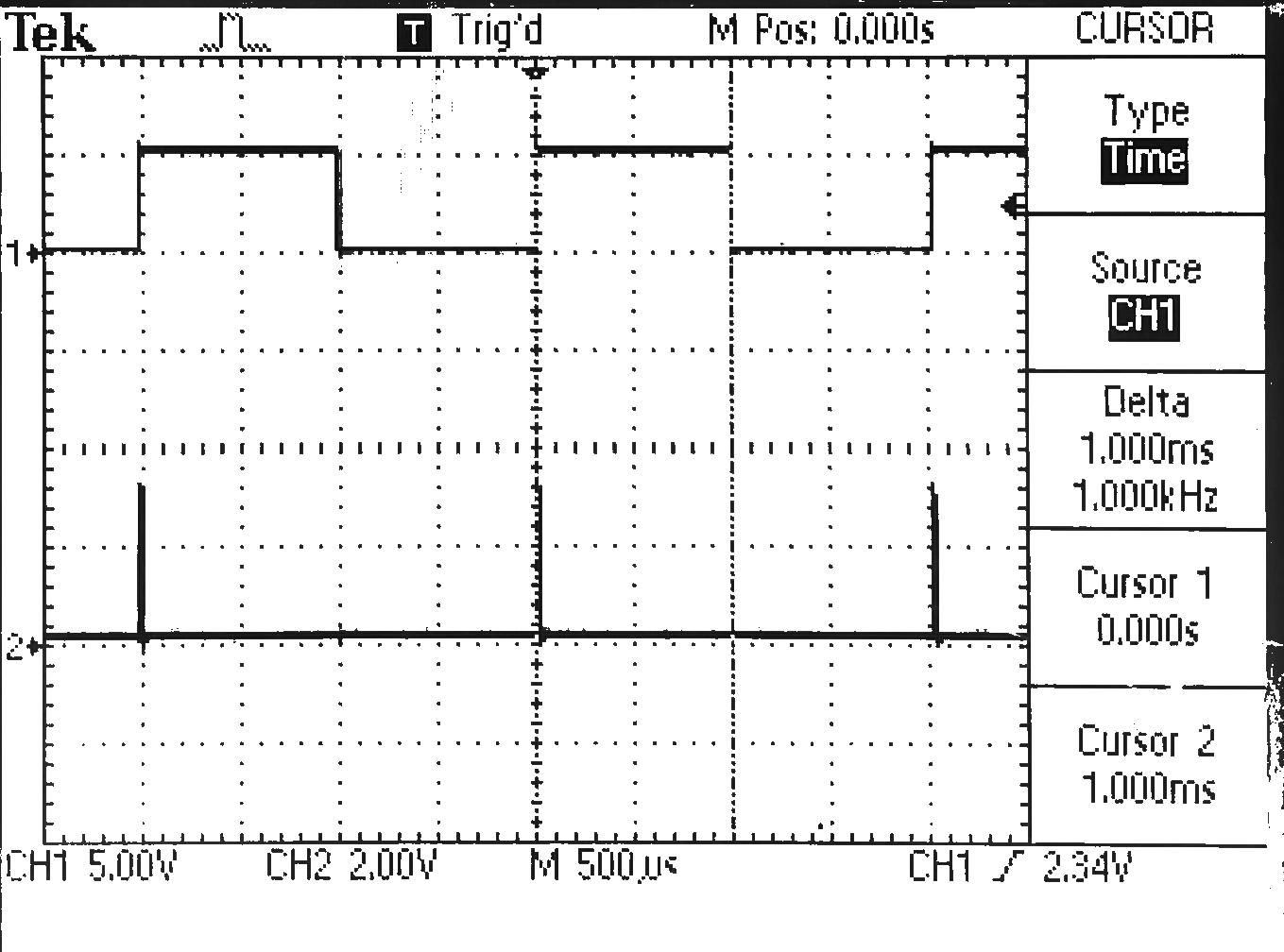
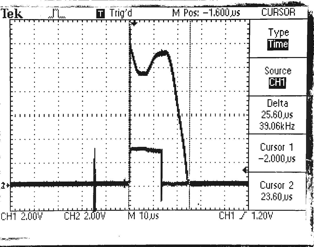
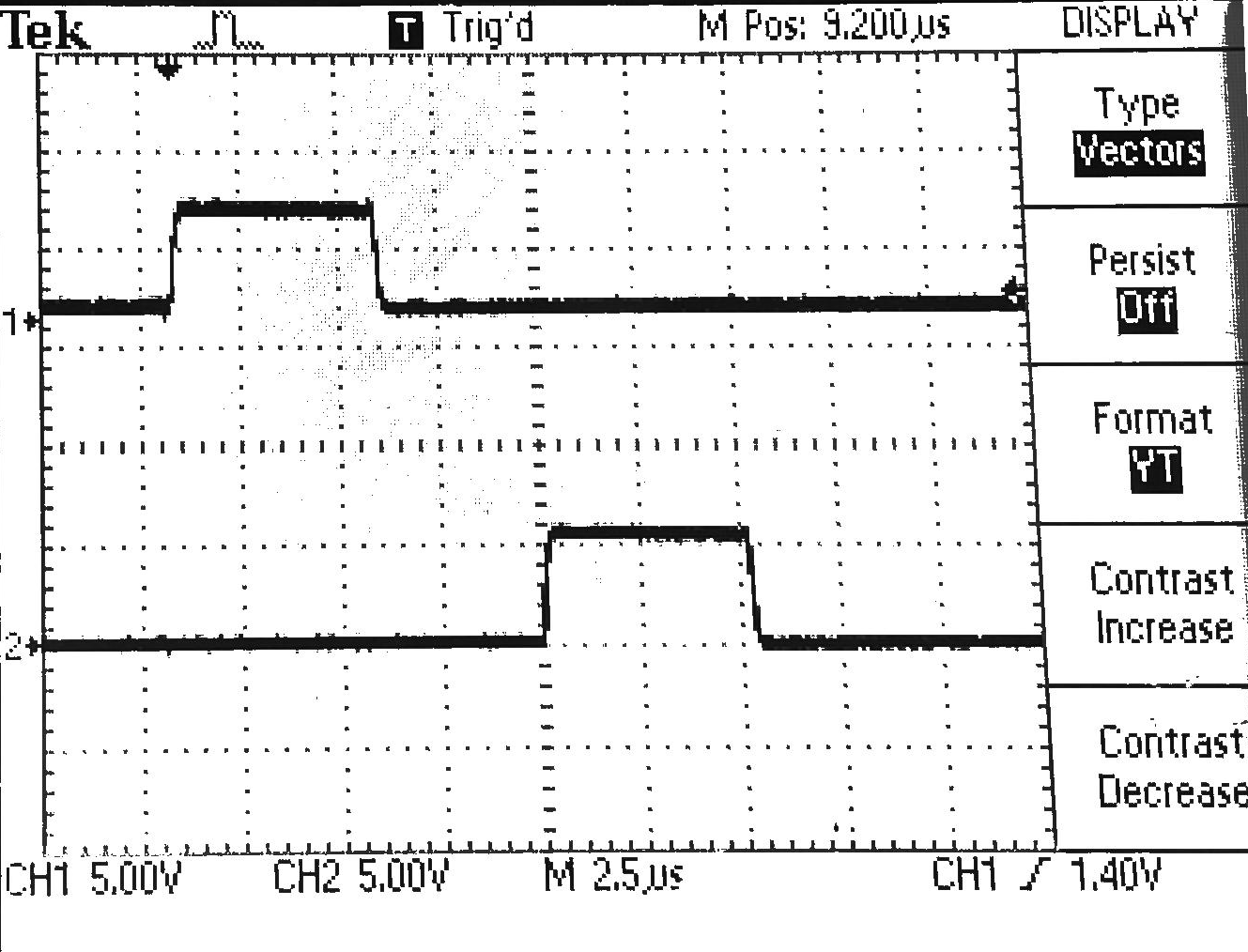
I've constructed the circuit on veroboard. Shown below is the PWM input signal (top) and the first output pulse from the timer IC below it on channel 2 labelled "pulse 1" in the schematic above.
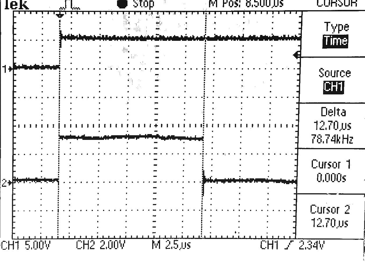
The first output pulse (width around 13\$\mu\$s) is shown relative to the rising edge of the PWM pulse:
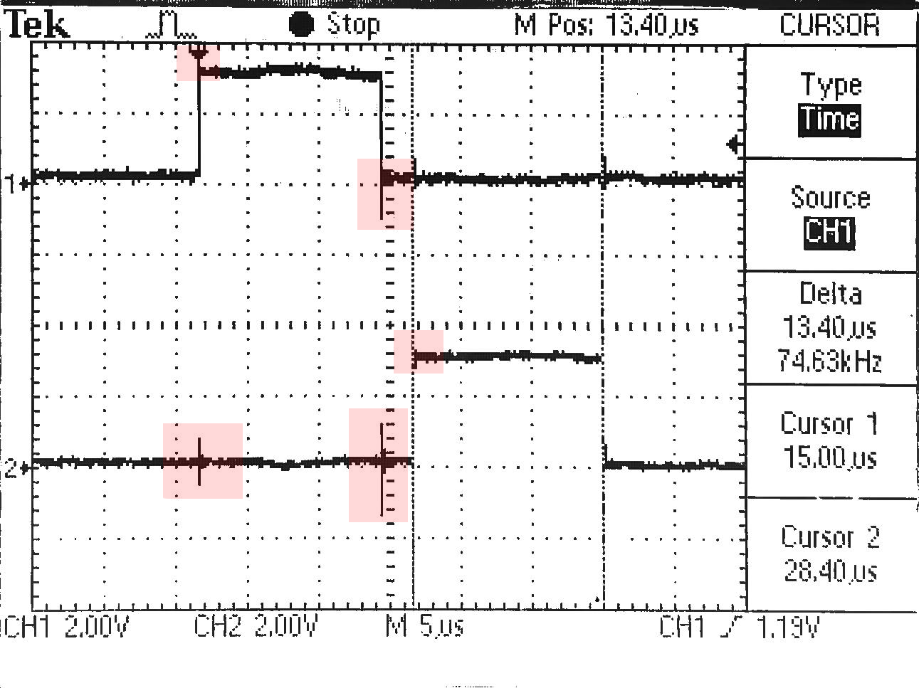
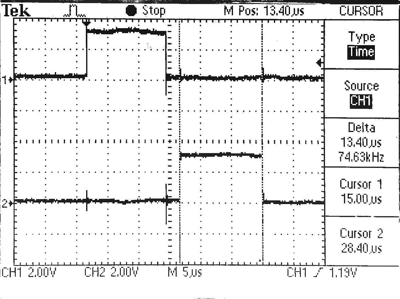
Lastly the first output pulse and second output pulse are shown top and bottom respectively. At the rising edge of pulse 1 there is a small spike on the second channel as well as a larger spike where the falling edge of pulse 1 is on the second channel. There are also some spikes at the pulse edges. I've highlighted these "trouble regions" in red below. Ordinarily this wouldn't be a problem however these pulses are fed into an H-bridge circuit and used to switch high voltages (I suspect that these pulses may be too small to drive such large voltages but that is another story) and so I need the pulses to be as square as possible and transition from low to high without any spikes before the rising edges. Using the second pulse from this timing circuit into my H-bridge amplifies this spike before the rising edge. This is undesirable for my application as I'm trying to use two consecutive small high voltage pulses to flex a piezo buzzer in one direction and then in another. This small pulse before the rising edge may cause the buzzer to flex in one direction, return to its nominal position and then flex again more strongly which I do not want:
My questions:
- What could be causing these small spikes before the rising edges?
- How can I remove those spikes and make these pulses as square as possible? (Schmitt trigger maybe?)
edit
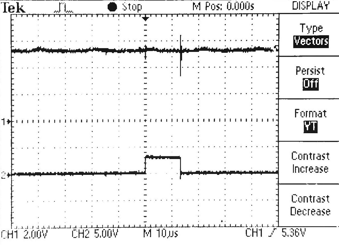
One user suggested monitoring the supply rails. Below is the 5V rail on channel 1 and on channel 2 the second output pulse from the timer. It looks like the +5V rail peaks and dips substantially (nearly 1V from nominal 5V) at the falling edge of the second pulse. On the veroboard I already have two 0.1uF caps from the VCC pin of each of the chips to ground. They're ceramic capacitors. The datasheet for this IC states:
VCC and ground wiring should conform to good high-frequency standards and practices so that switching transients on the VCC and ground return leads do not cause interaction between one-shots. A 0.01 mF to 0.10 mF bypass capacitor (disk ceramic or monolithic type) from VCC to ground is necessary on each device. Furthermore, the bypass capacitor should be located as close to the VCC-pin as space permits
- Tried changing the 0.01uF caps I had in there to 100uF but that made no difference to the spikes.

