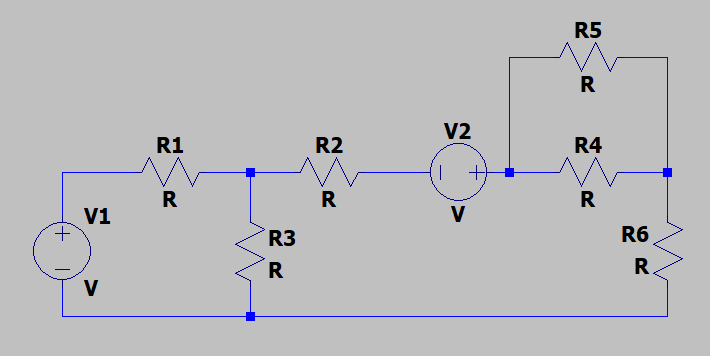
Unless you have a reason to do otherwise, it's a modern convention to use the negative lead of the battery pack or power supply as your ground node.
Unless you rely on actual physical properties of ground, eg, for radio, or to bond to a conductive housing, in a way it does not even matter.
Most uses chose the negative terminal, but a few legacy vehicles have had a positive chasis ground. And some long range telecom power feeds use positive ground under the idea that cathodes suffer less electrolytic degradation than anodes.
In terms of your circuit, the design is heavily inspired by the idea that the negative power supply will be ground and the reference point for all measurements. Notice how the components break up the positive paths, but not the negative, which is left consistent as a single node? It would be entirely possible to design a functionally equivalent circuit which instead maintained the integrity of the positive path for easy analysis relative to that, but it is not what the designer did. Hence we can see that the designer was displaying at least an unconscious, habitual assumption of the idea of a negative ground.
(One exception to the idea of circuit designs tilted towards ground integrity is the common use of semiconductor low side switches to switch the ground side of a load; even though it makes a circuit drawn from a negative ground perspective less clear, this is done because N-FETs are more efficient switches than their positive channel counterparts)


