0
\$\begingroup\$

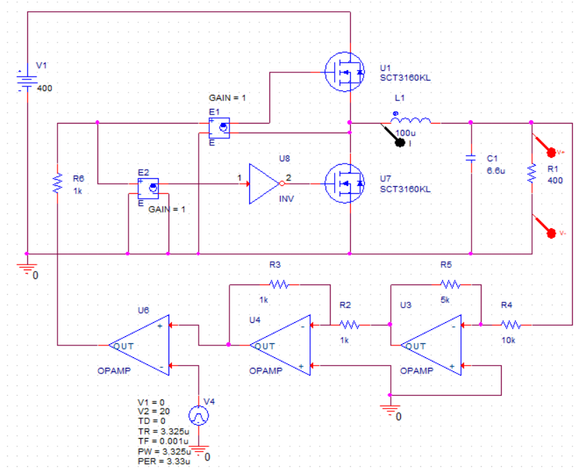
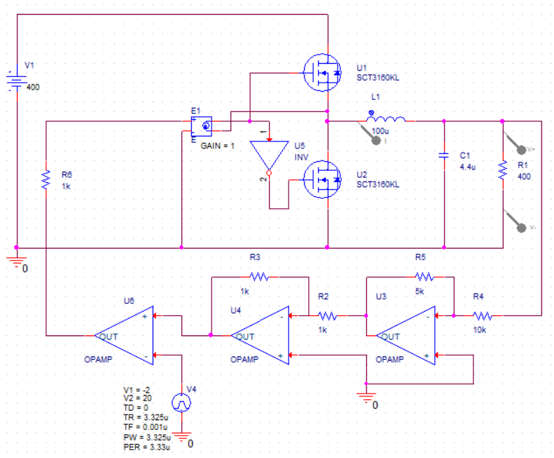
I'm trying to put my ZVS buck converter (DCM) in closed loop. I ran some simulations on MATLAB, and figured that just multiplying the transfer function of the open loop buck by 0.5 gives acceptable settling time, phase margin.

Now to implement this in the circuit, I used two inverting amplifiers, -0.5 and -1 (given by U3 and U4). The switching frequency is 300 kHz. So I tried to compare the output of U4 with the sawtooth wave of V4 whose period matches the switching frequency 300 kHz.

But I get a convergence error in Pspice. What am I doing wrong?

enter image description here

EDIT 1:- So I understood I made a mistake in the isolation of the gate pulse supplies,

enter image description here

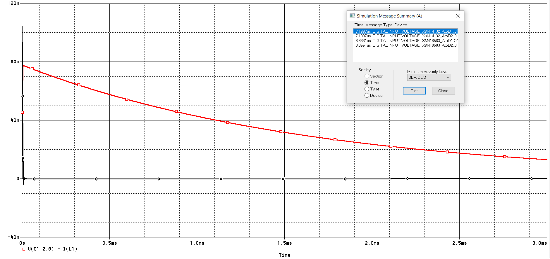
This is the erroneous result I am always getting:-

enter image description here

The output should be 200 V. I checked the feedback circuit was working or not by replacing U2 with a diode, and it didn't give me any errors, but I'm not sure this proves that the feedback loop is not the problem.

\$\endgroup\$
5
  • 1
    \$\begingroup\$ Before attempting to close the loop, I would first select a fixed bias at U6 (+) pin to have a 50% duty ratio for instance. Then, individually plot the gate-source voltage of each of the MOSFETs, you should have 0-10 V for a swing. Not sure you have that with a floating upper switch and the ground-referenced U5. When this works, then think about closing the loop. Check the polarity of the return path, it seems wrong and also, there is no gain or frequency compensation in your chain. \$\endgroup\$ Commented Apr 18, 2021 at 5:56
  • \$\begingroup\$ I need to get a constant 0.5 multiplied, that's why I put it as -0.5 and -1 to get +0.5. Wouldn't that work? And by polarity of return path do you mean U6 is wrong? Because I wanted to use U3 & U4 in inverting opamp configuration. \$\endgroup\$
    – SM32
    Commented Apr 18, 2021 at 6:12
  • 1
    \$\begingroup\$ Well, if the output voltage increases, the duty ratio must reduce for a negative feedback operation. Then, for a control system to operate, you need gain. Finally, the buck converter is a second-order system and there is usually a need for a frequency compensation of the return path. Check out my APEC 2019 seminar covering the buck converter. \$\endgroup\$ Commented Apr 18, 2021 at 7:41
  • \$\begingroup\$ I see. In my circuit, the gain needs to be 0.5, and since this is a DCM buck, I neglected the pole that's far away and thought it to be a first-order system. When I multiply the open-loop function with 0.5, I get the params to be acceptable.... \$\endgroup\$
    – SM32
    Commented Apr 18, 2021 at 10:25
  • \$\begingroup\$ There are many errors like: inverted logic - high output must lower duty, no error calculation according to reference voltage, feed 200v to amplifier is not a good way, feedback should be slowed with RC. \$\endgroup\$
    – user208862
    Commented Apr 18, 2021 at 19:10

1 Answer 1

0
\$\begingroup\$

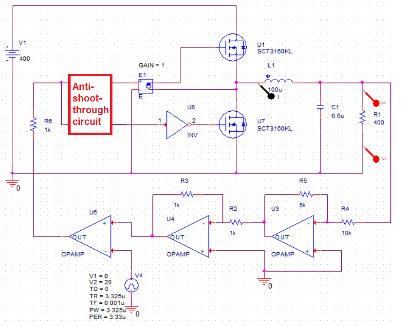
Your schematic will also need an anti-shoot-through circuit that prevents the two MOSFETs both being active at the same time. I've replaced the superfluous VCVS (E2) with that addition shown as a simple red block: -

enter image description here

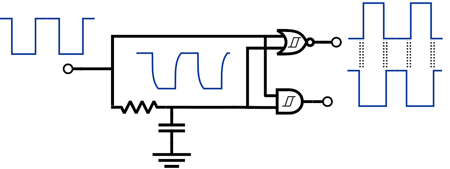
And, the actual additional circuit can look something like this: -

enter image description here

It provides a little bit of dead-time between one MOSFET turning off and the other turning on. That dead-time is controlled by the RC network shown above. Picture from here.

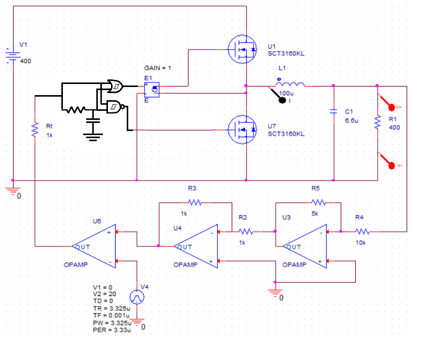
And, if you were implementing it in your circuit you could get rid of the inverter (U8) and do this: -

enter image description here

Note that I'm now using an OR gate and a NAND gate in the anti-shoot-through implementation above. You may need to play about with the implementation a bit to make sure I haven't introduced an inversion somewhere but that's fairly trivial.

\$\endgroup\$
6
  • \$\begingroup\$ Yes this is quite an important thing.I thought the NOT gate would ensure no shoot through. Alas, it still doesn't give the results. I think something is wrong with the feedback.(I need a constant gain of 0.5 so I used -0.5 and -1. I ignored the far-away pole and took it as a 1st order system.) \$\endgroup\$
    – SM32
    Commented Apr 18, 2021 at 15:21
  • \$\begingroup\$ @SM32 it looks like you have positive feedback. Try bypassing the unity-gain inverting amplifier. \$\endgroup\$
    – Andy aka
    Commented Apr 18, 2021 at 15:24
  • \$\begingroup\$ Unfortunately that didn't change the result I got with U4. I added the result I got. I tried with a diode in place of U2 and it worked, not sure what to think because it needs to be a synchronous buck. \$\endgroup\$
    – SM32
    Commented Apr 18, 2021 at 17:23
  • \$\begingroup\$ @SM32 sometimes you need to put more effort in to get things working. It's not all plain sailing. What do you mean regarding U2 - I see no U2? Did you bypass U4 correctly? Leave the diode in place and add the MOSFET and keep plugging away at things. It should work. Is your triangle wave peak voltage above the voltage you get from where U4 was connected? \$\endgroup\$
    – Andy aka
    Commented Apr 18, 2021 at 17:34
  • \$\begingroup\$ Sorry, I meant U7, the other MOSFET. I'll keep trying, thanks. \$\endgroup\$
    – SM32
    Commented Apr 18, 2021 at 18:15

Your Answer

By clicking “Post Your Answer”, you agree to our terms of service and acknowledge you have read our privacy policy.

Not the answer you're looking for? Browse other questions tagged or ask your own question.