2
\$\begingroup\$

I am trying to design a buck regulator with the following specification: Vin = 24V Vout = 5V I max = 8A Fsw=228k. The load is basically a long strip of RGB LED's. Which in certain cases would be all white for certain durations. I have measured these to be full white at 6.9A (hence 8A design).

I am considering the following high side FET: https://www.farnell.com/datasheets/2311812.pdf

And the buck regulator is LM25085A (https://www.ti.com/lit/ds/symlink/lm25085a.pdf?ts=1635166406663&ref_url=https%253A%252F%252Fwww.ti.com%252Fproduct%252FLM25085A)

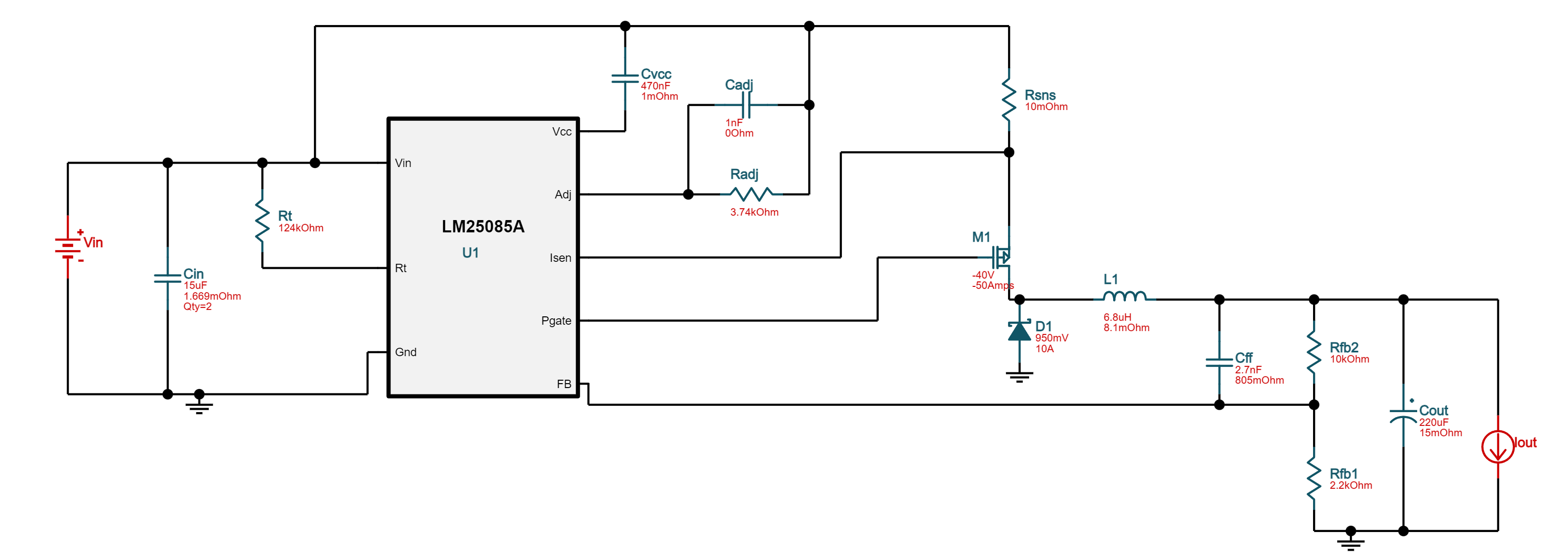
Here is a snippet of the design in TI webbench: enter image description here
I found the following equation for swithcing losses here (https://www.ti.com/lit/an/slyt664/slyt664.pdf?ts=1635224006712&ref_url=https%253A%252F%252Fwww.google.com%252F):

enter image description here Which if I try to calculate is 24 * 8 * 228k *((17n + 19n)/1.75A) = 0.9W. 1.75A is the source current going to gate and 1.65A is the sink current from the gate (values from LM25085) but for this example this value should be acceptable.

The continuous conduction loss is given as: enter image description here The datasheet for LM25085A suggests a good estimation for ripple as 20% of max load current so = 1.6A. RDSON is 45m from datasheet.

So that would be 45m * 5/24 * (8^2 +(1.6^2/12) = 0.602W

Total losses are therefore around 1.5W.

The only temperature value in the datasheet of the FET is channel to ambient and that is just 2.5C/W

So temp rise is 2.5* 1.5 = 3.75 degrees rise.

That sounds pretty low but I guess makes sense as the package is rated for 25A continuous current.

However, I then came across the following graph in the datasheet: enter image description here
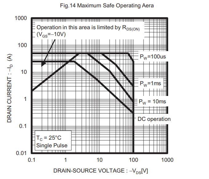
If I use the DC operation as a starting point, and VDS as max input voltage (24 V), it would seem the safe operating limit is 2A? I am not sure I understand this bit and whether the FET would work in such application? What pw value from the SOA graph should I be using?

\$\endgroup\$
5
  • 1
    \$\begingroup\$ I recommend that you review your recent questions (since April last year) and see if there are any that need completing by the usual procedure. You were good at answer acceptance in April BTW. \$\endgroup\$
    – Andy aka
    Commented Feb 7, 2022 at 19:13
  • 3
    \$\begingroup\$ The SOA curve is for linear application. Yours is not since you are switching. \$\endgroup\$
    – winny
    Commented Feb 7, 2022 at 19:29
  • 1
    \$\begingroup\$ Your seemingly low temp rise would apply on an infinite heatsink ,not a smd pcb , \$\endgroup\$
    – Autistic
    Commented Feb 7, 2022 at 19:54
  • \$\begingroup\$ @Andy aka done. \$\endgroup\$
    – Hasman404
    Commented Feb 8, 2022 at 9:00
  • \$\begingroup\$ @Autistic, how would I calculate a realistic temp rise value here with no more thermal impedance values shared. Or say with no heatsinking. Even if there was something more realistic shared like 1cm^2 copper heat sink. \$\endgroup\$
    – Hasman404
    Commented Feb 8, 2022 at 9:03

2 Answers 2

1
\$\begingroup\$

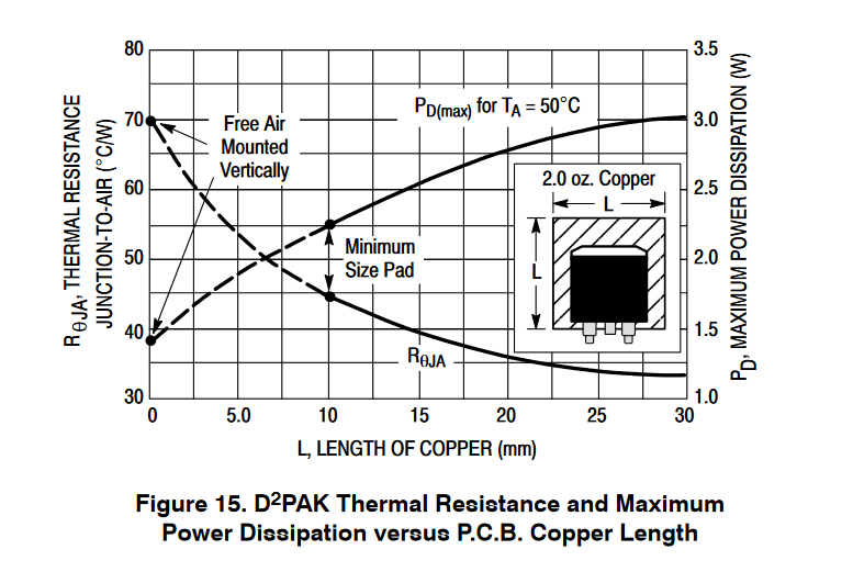
The thermal resistance of D2PAK depends on size of copper area under it.
See for example datasheet of MC78xx page 22: enter image description here If you designate copper area 20x20mm then the thermal resistance will be around 36 °C/W. Then you can calculate temperature rise for 1.5 W. It will be like 54 °C.

1.5 W is certainly going to make higher temperature rise than 3.75 °C. (for D2PAK a no heatsink)

SOA:
You are misinterpreting it. You cannot use current when mosfet is fully on, an voltage when mosfet is fully off.
If you consider mosfet fully on, you have to take the current and voltage across drain and source.
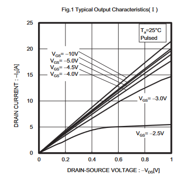
enter image description here

So for current 8A, the Vds is around 0.5 V. That is within SOA.

\$\endgroup\$
0
\$\begingroup\$

Double check your formulae for mosfet switching loss.Diode capacitance is not included and is significant .Your formulae implies that if the gate drive is perfect there will be no losses in switching .Stored capacitive energy is dissipated in a hard switch .I have discussed your formulae with others to confirm this .So your actual losses could be more than predicted .This is important because 40K per watt is a more reasonable value for your SMD mosfet on a normal FR4 PCB .I would say that your design will be thermal challenged .

\$\endgroup\$

Your Answer

By clicking “Post Your Answer”, you agree to our terms of service and acknowledge you have read our privacy policy.

Not the answer you're looking for? Browse other questions tagged or ask your own question.