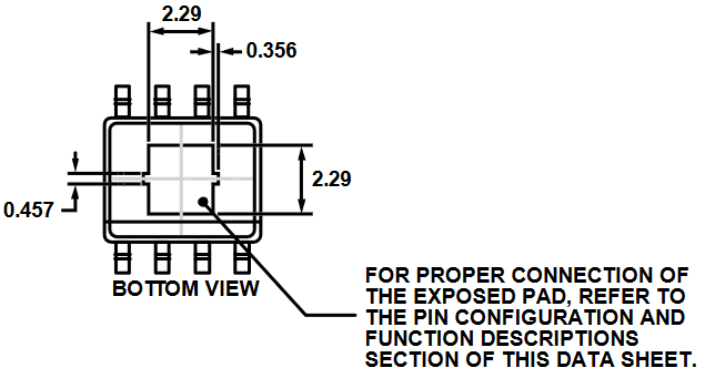
I've noticed a few component packages now that have small "tabs" on the sides of their exposed pad (thermal pad). One example is the Analog Devices ADM7154 LDO:
Note the 0.356 x 0.457 mm tabs on the left and right sides of the exposed pad.
- Why does the package have these tabs?
- Should the PCB footprint / land pattern also have these tabs?
- If so, and they're omitted from the PCB footprint, will this have any serious effects on reflow solderability, thermal or electrical performance?


