0
\$\begingroup\$

I have a footprint which provides VDD in two places on the board.

Specifically, it's a CR2032 battery retainer:

enter image description here

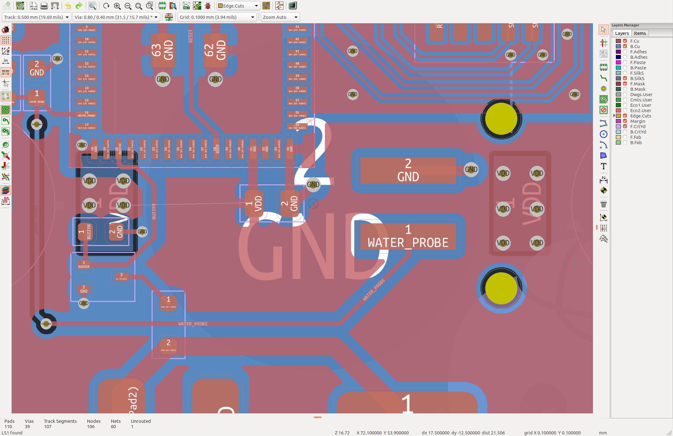
I then bring that VDD to the top with vias and I have a big pouring of that VDD.

However, that pouring is broken in 2. The left is not connected to the right.

If feel it's even better in some way because there is no VDD "loop" on my board, but it makes KiCad complain that it's somehow unconnected (you can see the little line between one of the VDD vias and the VDD pad of the decoupling capacitor in the middle of the image).

  1. Shouldn't KiCad know that it is connected through the footprint, as both pads have the same ID?

  2. I feel like ignoring this error, is this a good idea?

enter image description here

enter image description here

\$\endgroup\$
6
  • \$\begingroup\$ How is it represented schematically? \$\endgroup\$
    – Andy aka
    Commented Dec 18, 2022 at 14:25
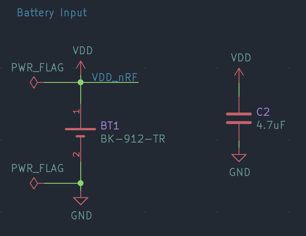
  • \$\begingroup\$ Let my know if it would be better to include the whole schematic, I added the battery section for now. \$\endgroup\$
    – Francois
    Commented Dec 18, 2022 at 14:31
  • 2
    \$\begingroup\$ Two pins with the same net means they need to be connected. As far as I know there is no way to tell kicad that pads are connected internally. I think you either ignore it or create two VDD nets (1 and 2) and note in the schematic that they're internally connected. If no one surprises me with a solution I'll type this up as an answer. \$\endgroup\$ Commented Dec 18, 2022 at 14:34
  • \$\begingroup\$ You need to show all the pins schematically and, link them all to Vdd. \$\endgroup\$
    – Andy aka
    Commented Dec 18, 2022 at 14:38
  • 1
    \$\begingroup\$ A bad way that works is to provide an ultrafine track that will always edtch away - the manufacturer needs to know about this. || Another way is to have a track with a hole drilled in it - manufacturer also needs to know. \$\endgroup\$
    – Russell McMahon
    Commented Dec 19, 2022 at 8:07

3 Answers 3

3
\$\begingroup\$

In answer to your two questions:

1. Shouldn't kicad know that it is connected through the
   footprint as both pads have the same ID?

The short answer is 'no' because this breaks testing assumptions for board manufacturers that do e-tests. For a longer answer with some discussion about how KiCad might address this in the future, you can can read the related issue report at https://gitlab.com/kicad/code/kicad/-/issues/2558

2. I feel like ignoring this error, is this a good idea?
This is the correct solution with KiCad version 6.

\$\endgroup\$
2
\$\begingroup\$

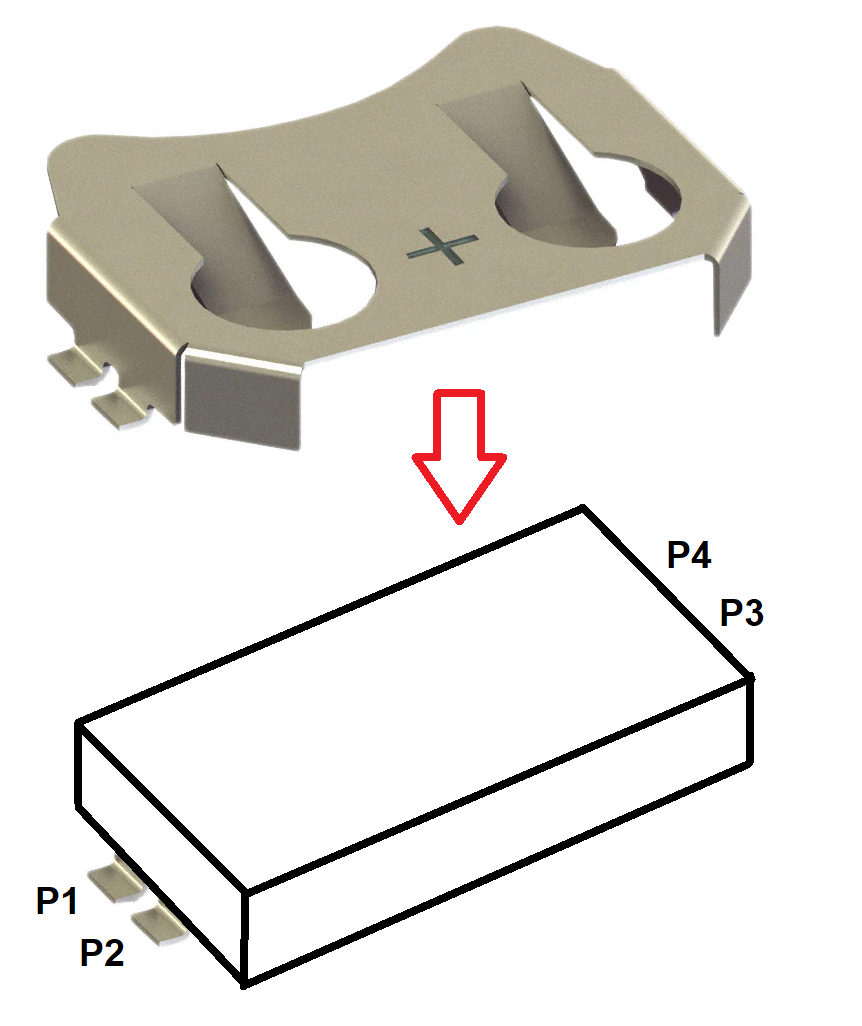
You need to regard the battery holder as a 4 pin device like this: -

enter image description here

Then, connect all four pins to Vdd in your schematic.

Just regard it as an IC (in other words).

\$\endgroup\$
2
\$\begingroup\$

Two methods, neither of which is "good practice", and both of which work, are:

  • Provide an ultrafine track that will always etch away.

  • Have a track with a hole drilled in it.

The manufacturer needs to know that either of these actions are intentional if used.
Only do things like this if "proper" solutions are for some reason impractical.

\$\endgroup\$

Your Answer

By clicking “Post Your Answer”, you agree to our terms of service and acknowledge you have read our privacy policy.

Not the answer you're looking for? Browse other questions tagged or ask your own question.