It seems to be a bespoke and inexperienced design. The thought process seems something like:
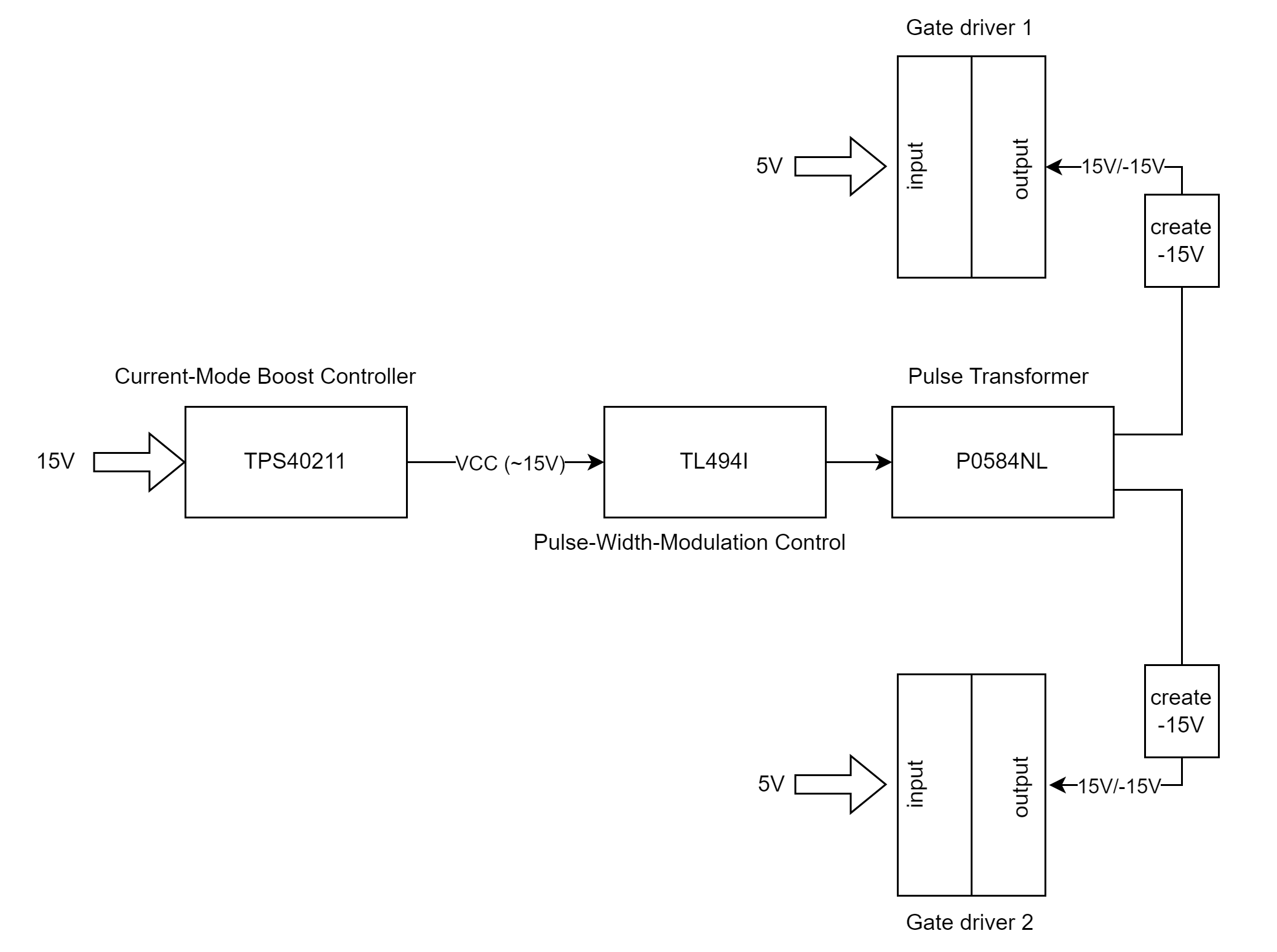
1. We need +15/-5V at the gates.
(My assumption, since the gate drive section isn't shown.)
We can make -5 by regulating down (er, up) -15. And we can make +/-15 by rectifying a 15V square wave.
Catch: the rectifiers drop a volt or so. And the drive transistors, another one or two.
So let's boost the input up to 17V or so.
2. We need something to make that square wave.
Drop in a TL494, those make square waves right?
It appears to be hard-wired for fixed duty cycle, so there's no PWM going on here. There's also no* current limiting, it's hard switching into the output filter caps (labeled as "100pF" but I'm guessing they're at least a few µF in actuality?). It would be a forward converter, but there's no filter choke. It would be a charge pump, but there's no series capacitor to pump charge through; instead it's transformer coupled. It's the worst of both worlds...
*The TL494 can only sink 200mA or so, if you don't mind that its power dissipation goes way up when forced into current limiting. Normally a series inductance (the transformer itself in a flyback converter, or the choke-input filter in a forward converter) limits dI/dt and therefore PWM can be varied to control output or peak current. But with fixed PWM, this is not possible here.
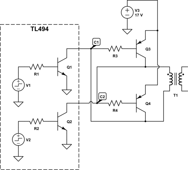
The equivalent circuit looks something like this:

simulate this circuit – Schematic created using CircuitLab
I think you had Q3/Q4 correct the first time.
Q1 and Q2 are Darlington style internally, hence the higher voltage drop. When Q1 is on, Q3 is also on, and T1 has positive voltage drop; when Q2 is on, Q4 is on and T1 has negative voltage drop. It's a simple H-bridge arrangement.
Note that Q3/Q4 are not turned off very well: the C1/C2 voltage is only pulled up to VCE(sat) below VCC, which could be a significant drop under load current. R3/R4 are fairly large so the reverse base current will be small; a B-E resistor would be welcome, to improve turn-off and reduce cross-conduction. Perhaps the TL494 is set to low enough duty cycle that this isn't a problem; I didn't check. (At IB(off) = 0, typical BJTs take about 10µs to turn off on their own. Probably it's under 1µs here.)
TL494 is a full (if primitive) SMPS controller, so it's a bit of a waste here. But it's cheap, and not much different in size from, say, a CD4047B, or a SN6501 plus cascode transistors.
3. We have 15V input, but need 17.
Maybe the input is variable as well, I don't know (could be a battery, unregulated (linear) supply, long wires, etc.). The boost covers for a few possibilities.
TPS40211 is a poor choice, but that may itself be a mistake that was only discovered by doing. I've made this mistake myself... The problem is, its error amplifier output range overlaps the fault threshold, so it can't ever go into current limiting without faulting (stopping and restarting). It can soft-start once, and that's it.
I'm guessing Q3 is misidentified and actually an N-MOSFET. I suppose a BJT could be used, but R14 should be a different drive network, and even then, most gate drivers aren't rated for much DC output (which isn't to say they can't deliver it reliably, just that you don't know for sure).
UC3843 (and family) and LM3481 are better options for controllers; for regulators, CS5171 (and family), NCV3063 (and family); even MC34063 wouldn't be terrible here but it is rather slow so requires larger capacitors and inductor than others. And myriad others I don't know offhand; probably lots in SOT-23-5 and up. Also at these low power levels (assumption), some boost type LED/backlight regulators could be (ab)used if you really had to.
What Should've Been Done
Just one transformer, flyback is fine, individual windings for each output. This may need to be a custom part, but there are (somewhat roundabout) solutions using multiple single transformers / coupled inductors, wiring the primaries in parallel. And if you don't find the right inductance and coupling factor, that's not a show stopper either: magnetizing inductance can be wired in parallel with the primary, allowing the use of generic pulse transformers.
Regulation can be based on the primary side, with a little care to avoid the overshoot due to leakage inductance. Or one output can be chosen as priority, and a TL431 error amp and optoisolator connected there. (Cross-regulation shouldn't be important as the gate drivers will all be active at the same time (assumption).)
If this is the usual +15/-5V gate drive that many IGBTs require, I would opt for a flat 20V output, and shunt regulate the "0V" with a zener. The logic isolator and gate driver will be common-ground to the negative side, and the IGBT emitter ties to the "0V" zener node. No DC flows through the gate normally, so very little bias is needed in the zener; a mA should be plenty. Generous bypass caps shall be used, to ensure gate charge doesn't shift around the "0V" node. Say, 10uF from +15 to 0, and 0 to -5. Which can also serve as local bypass for the driver, no big deal.
So that basically cuts the circuit in half, or less. Easy optimizations with a little thought; like I said, my guess is the original designer was inexperienced, perhaps rushed, and ended up accumulating a design rather than considering it holistically.
Some final tips:
If this is a lower power application (say, DC link up to 500V, load current up to 20A, give or take), bootstrap gate drivers may suffice, and then isolated supplies likely aren't required. (If the output needs to be DC stable (0/100% duty cycle), isolated DC-DC for the high side is still a good idea. Under 100V or so, a charge pump can be used.) The bipolar gate drive will be harder to arrange, but at lower power levels, MOSFETs are more attractive and suitable with unipolar (e.g. +12/0V) gate voltage.
If you are [re]designing much more of this system than just the driver, include desat protection! That is, a circuit that monitors VGE and VCE such that, if VCE rises significantly above VCE(sat) (say, a few volts) while VGE is "on", transmit a "panic" signal backwards across the isolation barrier (use a two-channel bidirectional logic isolator, or two optos). At the controller, latch this signal into a fault and disable the outputs -- quickly, within 10µs. The main downside to desat protection is nuisance tripping; it has to be delayed (slowed, filtered) enough that it doesn't trigger all the time (a little hard switching is usually necessary, i.e. turning on VGE while VCE is initially high), but not by so much that, in a short-circuit event, the transistor is destroyed (usually 5-20µs is the survival limit). For a more integrated solution, consider ACPL-330J: pricey, but has everything you need, and you'll pay about as much for a more discrete solution.
(Desat protection can also be used with MOSFETs! You may need a higher voltage threshold, depending on RDS(on), of course.)


X?missing a DC return path? \$\endgroup\$