The rotary encoders I'm using are sold with several different output options. Analogue sinusoidal (90* phase shifted sin and cosine signal), Incremental output (90* phase shifted quadrature signals with a third signal as a reference), or SSI (similar to SPI, but no chip select line). I need to send the signal from the encoders to a single pin on the computer, which can either be SPI, UART, or CAN. Right now, my outline for solving this problem is to send the signal from each encoder to either an ADC converting it to one of those three protocols and then sending that signal to a multiplexer to output on a single line, or converting the SSI to SPI artificially and multiplexing that signal. I am not sure either is a sound solution since that signal needs to have reasonably low latency - those positions will be used for controlling some motors elsewhere in the system. The controller also needs to receive positions corresponding to the same instance in time, which I've only got a foggy idea of how I might accomplish this.
-
1\$\begingroup\$ How do you plan on doing SPI with a single pin? Even with one-way communication and no chip select line you'd at least need data and clock to make it be any semblance of SPI. I'm less familiar with CAN but suspect a similar problem would limit you there. \$\endgroup\$– HearthCommented Feb 7, 2023 at 16:37
-
\$\begingroup\$ an analog multiplexer may work ... multiplex the two analog signals, plus a third DC voltage to act as a sync signal ... set the DC voltage outside of the encoder range \$\endgroup\$– jsotolaCommented Feb 7, 2023 at 16:56
-
\$\begingroup\$ How often do you need updates? Do you need samples at the same time for each encoder? \$\endgroup\$– Scott SeidmanCommented Feb 7, 2023 at 17:06
-
\$\begingroup\$ Personally, I might consider a separate decoder for each channel that sends digital data to a single unit \$\endgroup\$– Scott SeidmanCommented Feb 7, 2023 at 17:08
-
\$\begingroup\$ What's the part number for the rotary encoders? That'll tell us a lot about the parameters you're working with. \$\endgroup\$– PolynomialCommented Feb 8, 2023 at 2:03
1 Answer
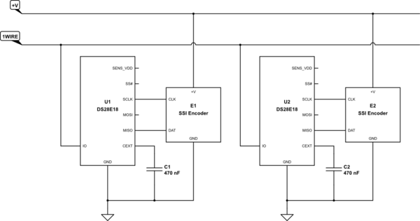
The easiest way to read three SSI encoders over a single pin would be via interface ICs using a 1-Wire bus.
You could use three DS28E18 1-Wire to I2C/SPI bridge ICs in SPI mode, e.g. as follows:

simulate this circuit – Schematic created using CircuitLab
Repeat for as many encoders as you need.
The DS28E18 ICs are powered directly from the bus, storing energy in the 470nF capacitor, so you don't need to supply them with any power. The DS28E18 is a 3.3V device so you may need to perform logic level translation between it and the encoders if they require 5V IO.
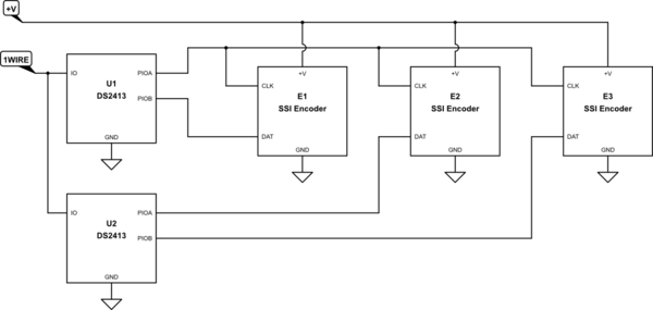
Another alternative is to bit-bang everything with a 1-Wire GPIO expander (or several). A pair of DS2413 Dual IO expanders would work here, giving you four IOs: one for clock output, the other three for reading the SSI data back.

The DS2413 ICs are also bus-powered, and also have an internal capacitor so you don't need to add one. In this configuration you would set U1's PIOA as an output and the other 3 pins as an input. You'd toggle U1.PIOA high and low repeatedly as a clock signal. After each toggle high, you'd read the other 3 pin values, and bit-shift them into three integer values. On a 16-bit encoder you'd repeat this 16 times until you've read 16 bits from each encoder.
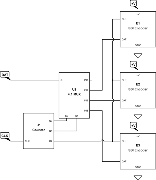
If you can spare two GPIO pins instead of just one, you could use a counter and a multiplexer:

The CLK input on the left is a clock signal generated by your MCU. This clock signal will toggle between reading the different encoders, and will also be used to derive the SSI clock.
The bottom two bits (Q1, Q0) of the counter will count up (00, 01, 10, 11) on each clock cycle. These two bits set which of the four multiplexer inputs are read. Since you only have three inputs to read, we leave the first input disconnected and just ignore it. The third counter bit (Q2) will flip on every 4th cycle, i.e. creating a divide-by-8 clock signal to drive the SSI clock for the encoders.
On startup, send 3 clock pulses into CLK. This sets things up so that the next clock pulse will cause a rising edge on the SSI clock and set the mux address to 00.
Now, every time you want to read from the encoders, you follow this procedure:
- Send two clock pulses.
- Read the value on DAT. This will read one bit from the first encoder.
- Send another clock pulse.
- Read the value on DAT. This will read one bit from the second encoder.
- Send another clock pulse.
- Read the value on DAT. This will read one bit from the third encoder.
- Send four clock pulses. This gets us back to our starting condition.
- Repeat all of these steps for as many bits as you need to read from the encoders (e.g. 15 more times if you have a 16-bit encoder)
I made a simulation of the circuit here so you can follow along with what's happening.
The first three clock pulses increment the counter to 011, so the mux address is set to 11. The first clock pulse in step 1 causes the counter output to go to 100, which results in a rising edge on the SSI clock and the mux address being set to 00 (selecting the disconnected IN0 input). The rising edge on the SSI clock causes the encoders to output their first bit. On the second clock pulse of step 1, the counter output goes to 101, which selects mux input IN1. You then read back a value. On the clock pulse in step 3, the counter goes to 110, which selects mux input IN2. You read back another value. On the clock pulse in step 5, the counter goes to 111, which selects mux input IN3. You then read the final value. In step 7 you send four clock pulses. On the first pulse, the counter wraps back to 000. The next three pulses set the counter output to 001, 010, and finally 011, which is back to the initial state we had before step 1, ready to read another set of bits.
