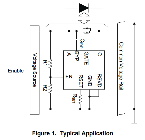
I have recently integrated an ideal diode circuit based on the TPS2419D chip from TI.
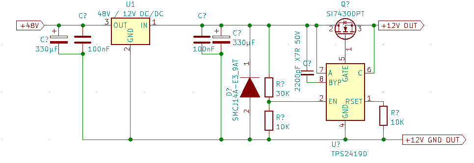
The schematic is the following:
When I apply 48 V to the input of the DC/DC, I do get 12 V at the output of the DC/DC, but almost nothing at the output of the ideal diode.
I've probed the values in this phase and they are like this :
- pin1 (RSET): 0 V
- pin2 (EN): 3.017 V
- pin3: 0 V
- pin4 (GND): 0 V
- pin5 (GATE): 0 V
- pin6 (C): 0.1 V
- pin7 (A): 12 V
- pin8 (BYP): 10.88 V
As I've discovered (not on purpose), if I shunt pin 6 & pin 7 briefly, the circuit will "wake-up" and I get 12 V at the output.
I've put a mild load (0.5 A) and it seems to work, but as soon as I unplug it the circuit has to be "woken up" again.
I'm a bit lost so any leads will be appreciated.
ADDENDUM (15/03/23) :
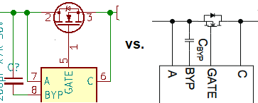
After @Tom-Carpenter pointed out that my FET was the wrong way around, I managed to cobble a test circuit together.
However, the circuit remains unfunctional.
- the FET might have been damaged in the rework process but I doubt it.
- I now obviously get a voltage at the output of the MOSFET all the time at the +12 V out, but it's more than likely the body diode conducting since I get a steep voltage drop (11.4 V with 12.05 V before the FET) even at very low current. Also, the gate voltage is only 12 V (referenced to ground) so Vgs is not where it should it be, correct?
- The voltage at pin 8 (BYP) is 22 V so it seems like the bootstrap/charge-pump is working, but why doesn't it drive the gate?
- Last but not least: when I use it as a blocking diode (U_post_mosfet > U_pre_mosfet), the MOSFET heats up quite quickly and I get a rapid clicking noise (2 Hz maybe), not exactly the behaviour I expected.


if I shunt briefly the pin 6 & pin 7, the circuit will "wake-up"... what makes you think that the circuit wakes up? ... connecting pin 6 to pin 7 bypasses the MOSFET, therefore the circuit is bypassed \$\endgroup\$