0
\$\begingroup\$

I've decided to simplify my previous "solid-state switch" that has to switch 5A @ 60V.

Instead of using an N-channel MOSFET plus a gate driver (which has to have a charge pump in order to have 100% duty cycle, I learned the hard way,) I plan on using a P-channel MOSFET directly driven by a GPIO.

I'm unsure about the way to treat that since the GPIO is 12V tolerant but the P-channel switches 60V.

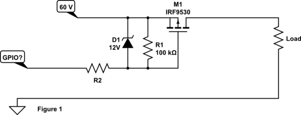
The GPIO when high brings its output to the ground and stays floating when low. I've added the 100K pull-up resistor to be sure the FET stays off when not driven but does that compromise the GPIO by also pulling it to 60V?

Having that in mind, I copied another schematic and added a 12V Zener in order to clamp that voltage but at the same time, won't that defeat the purpose of the pull-up resistor since Vgs will always be <0 in that case??

schematic

simulate this circuit – Schematic created using CircuitLab

\$\endgroup\$

1 Answer 1

2
\$\begingroup\$

The resistor R1 ensures that the voltage from source to gate (\$V_{SG}\$ )will be zero volts under open circuit. It brings the gate to the same potential as the source. The zener diode clamps \$V_{SG}\$ to 12 V but what will protect the zener from over voltage or excessive current?

The node labeled "GPIO12V" limited is not limited to 12V. It must range from 60 V to between 0V and 48V.

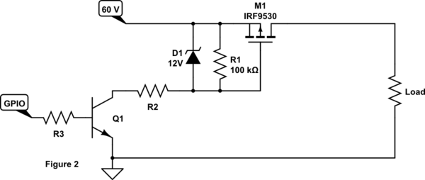
But the source-gate voltage will be limited to 12 V but only if there is a series resistor as shown in my first diagram below.

The added resistor R2 will prevent excess current through the zener diode when the switch input is low. The node labeled "GPIO?" iidicates that a ,odern MCU GPIO cannot handle the voltage range. The node must switch between 60V and OV to operate the switch. A level translating transistor is required as shown in my second diagram.

Choose R2 for proper zener current,

Choose R3 for proper base current, enough to drive Q1 into saturation. Well .. it needs to turn on enough to bring the zener diode anode to < 48 volts.

schematic

simulate this circuit – Schematic created using CircuitLab
schematic

simulate this circuit


Update:

However that does invert the signal, doesn't it? I'd like to keep the logic as is so, should I add another PNP stage in order to to do so?

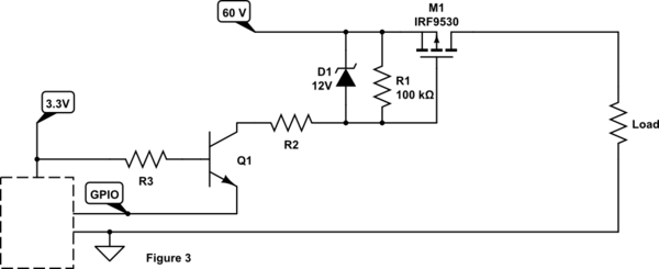
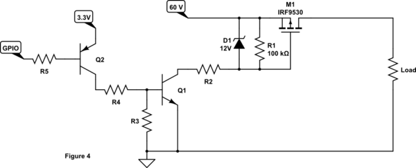
Figures 3 and 4 will allow the polarity to remain as the original.

The MCU GPIO in Figure 3 must be able to absorb the current passing through D1, but otherwise is a good choice.

Figure 4 uses a PNP transistor to invert the signal.
R3 can be high. It is there to hold the base at 0V when the Q2 is off.
R4 is chosen for the correct base current in Q1.
R5 is chosen for the correct base current in Q2.

schematic

simulate this circuit

schematic

simulate this circuit

\$\endgroup\$
4
  • \$\begingroup\$ I only see one diagram. \$\endgroup\$ Commented Mar 15, 2023 at 1:52
  • 1
    \$\begingroup\$ @evildemonic Finger trouble. Now there are 2. Thanks \$\endgroup\$
    – user319836
    Commented Mar 15, 2023 at 1:52
  • \$\begingroup\$ @RussellH Thank you for the schematic. However that does invert the signal, doesn't it? I'd like to keep the logic as is so, should I add another PNP stage in order to to do so? \$\endgroup\$ Commented Mar 15, 2023 at 12:51
  • \$\begingroup\$ See my update @VoltsAndNuts. \$\endgroup\$
    – user319836
    Commented Mar 15, 2023 at 19:05

Your Answer

By clicking “Post Your Answer”, you agree to our terms of service and acknowledge you have read our privacy policy.

Not the answer you're looking for? Browse other questions tagged or ask your own question.