5
\$\begingroup\$

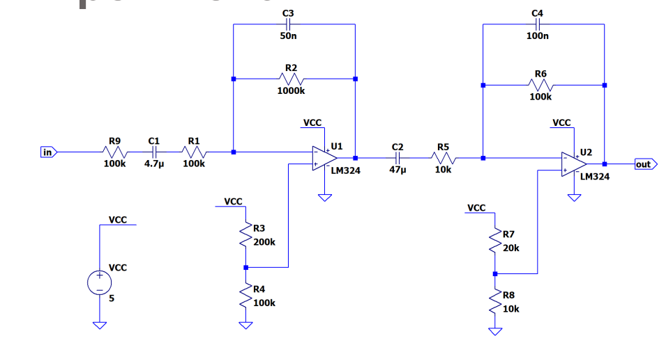
I know my question is a bit broad, but I want to ask: Using the single supply configuration, why does the first stage's non-inverting input and second stage's non-inverting input use different voltage dividers, the first one being: 200k ohm and 100k ohm, the second one being 20k ohm and 10k ohm.

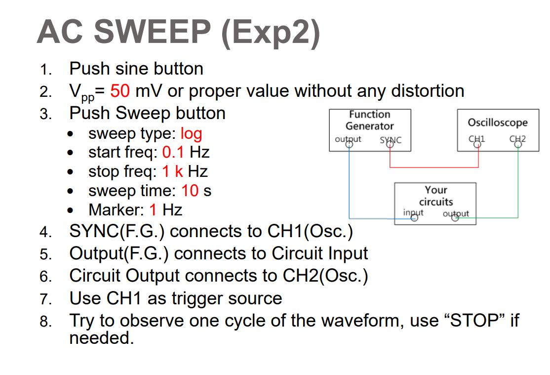
edit: the input signal is shown as above: using a function generator to perform an AC sweep

\$\endgroup\$
5
  • 1
    \$\begingroup\$ I initially thought the designer might have wanted to have equal resistance looking out from each input of each op-amp to minimize errors due to input bias current, but the blocking capacitors C1 and C2 mean they've badly missed the mark if that was their intent. \$\endgroup\$
    – The Photon
    Commented Apr 30, 2023 at 6:09
  • \$\begingroup\$ @ThePhoton I would undelete your answer as I think it is indeed the most likely origin. Both reason and failure. \$\endgroup\$
    – tobalt
    Commented Apr 30, 2023 at 6:21
  • \$\begingroup\$ Incompetent designer I would say. Maybe you should say where the picture came from. \$\endgroup\$
    – Andy aka
    Commented Apr 30, 2023 at 9:36
  • \$\begingroup\$ it is the electronic lab I did last week, I don't know exactly who designed it, but it is this lab is mainly about making a "low budget heart rate monitor", the input signal after doing the ac sweep will be changed to a infrared LED driver(LTH1550-01, datasheet: pdf1.alldatasheet.com/datasheet-pdf/view/194716/LITEON/… ) circuit, and I will put my finger on the LTH1550-01 sensor, and that heart rate signal will serve as the input signal to the two band-pass filters. \$\endgroup\$ Commented Apr 30, 2023 at 10:13
  • \$\begingroup\$ Both resistive dividers yield similar DC voltage for their respective "+" input. Perhaps their somewhat redundant duplication aids troubleshooting...you can build this one stage at a time and probe each stage independently. The DC offsets caused by R3, R4 and R2 are fairly minor. Because of AC-coupling via C2, U1's DC offset is blocked, so it isn't such a terrible design from a biasing point-of-view. \$\endgroup\$
    – glen_geek
    Commented Apr 30, 2023 at 13:12

1 Answer 1

8
\$\begingroup\$

It looks like a case of (roughly) wanting to balance the resistance seen by each input of the two op-amps in order to minimize errors due to the input bias current. However, they have not done this correctly.

If it weren't for the blocking capacitor C1, the inverting input of U1 would see the equivalent of 100 kohms parallel with 1 megohm, which the designer roughly equaled by setting up the non-inverting input to see a Thevenin equivalent source with 100 kohms parallel with 200 kohms.

Similarly, if not for blocking capacitor C2, the inverting input of U2 would see 10 kohms parallel with 100 kohms, and they roughly equaled that by attaching 10 kohms parallel with 20 kohms to the non-inverting input.

Matching the resistance seen by the two inputs ensures that bias current effects affect both inputs equally, so that no differential input voltage is generated that would be amplified at the op-amp output.

However, with the blocking capacitors present, these calculations are all changed completely, and the resistances set up for the non-inverting inputs are not well-matched at all to what's seen on the inverting inputs.
\$\endgroup\$

Your Answer

By clicking “Post Your Answer”, you agree to our terms of service and acknowledge you have read our privacy policy.

Not the answer you're looking for? Browse other questions tagged or ask your own question.