2
\$\begingroup\$

Can someone explain in simple terms how a delta-sigma modulator works specifically for ADC applications? I've googled around and have been piecing it together but am still unclear on a few things.

Most descriptions note an accumulator with a certain DC offset that affects ADCs oscillation but I don't understand what is being accumulated/what is oscillating/ what threshold these are referring to.

\$\endgroup\$
3
  • \$\begingroup\$ How are you on conventional ADCs like successive approximation - these can be used in SD ADCs? What about analogue integrators and comaparators? Flip-flops - are you OK on these? I ask because it helps to understand where your level is before answering. \$\endgroup\$
    – Andy aka
    Commented Apr 29, 2013 at 14:49
  • \$\begingroup\$ I wrote about making an ADC on my blog. It isn't a strict Delta-Sigma ADC, but it is close. There could be some good info on that for you. davidkessner.wordpress.com/2011/05/01/adc-in-an-fpga \$\endgroup\$
    – user3624
    Commented Apr 29, 2013 at 17:10
  • \$\begingroup\$ I'm trying to learn analog integrators and voltage comparators right now. Flip Flops I am familiar with, same with successive approximation. \$\endgroup\$
    – Jessica
    Commented Apr 30, 2013 at 21:12

4 Answers 4

9
\$\begingroup\$

I think the easiest way to start thinking about this question is to imagine a "perfect-in-all-other-ways" parallel 8-bit ADC; it produces an 8-bit number every time it converts. It's an 8-bit device so it only approximates to the real analogue input fed to it.

Let's say it's input span is 0 to 2.55V - each lowest bit change is worth 10mV and 10mV is its resolution and accuracy (remember it's perfect in all other ways). If you inputted 1.015V, it would produce a digital output the equivalent of 1.01V i.e. there is an error of 5mV.

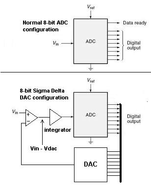
Now consider this situation: the ADC output is converted back to analogue by an 8-bit DAC and subtracted from the input voltage to produce an "error" voltage. Consider also that the error voltage is integrated and now feeds into the ADC's input instead of the original input.
enter image description here

What now happens is the the output of the ADC will hunt above and below the precise value of the real input voltage. Several consecutive ADC outputs can now be averaged (in the digital domain) to get a progressively more accurate picture of the real analogue signal.

Why not use a 4-bit ADC? If 4-Bits is used, to achieve the same accuracy as the 8-bit ADC, more consecutive results need to be averaged to accomodate the chunkiness of 4-bits compared to 8-bits.

Take this to extremes - imagine a one-bit ADC - basically it's a comparator - plenty of results need to be taken and averaged to reach the equivalent of an 8-bit ADC but if the speed is high and the processing power is good then no problem.

The difficulty explaining this type of ADC is that if you "use" the the normal Delta-Sigma single-bit architecture, the digital numbers produced can befuddle the mind. Anyway that's my take on things!

\$\endgroup\$
6
  • 1
    \$\begingroup\$ What's the purpose of the integrator in this circuit? \$\endgroup\$
    – Jessica
    Commented Apr 30, 2013 at 21:13
  • 1
    \$\begingroup\$ @Jessica the integrator is soooo important. Glad you focussed on it - after the ADC has approximated the real input (say 5mV low), this value is subtracted from the real input which leaves "the error" (+5mV) as the remainder - the integrated error pushes the ADC to produce a new "number" that has to be higher than the original input. This in turn produces -5mV as the error and this pulls the integrator down from where it was causing the ADC to produce a number lower than the real input and the cycle repeats. Thus an 8-bit ADC produces a 9-bit answer over two samples. \$\endgroup\$
    – Andy aka
    Commented Apr 30, 2013 at 21:28
  • 1
    \$\begingroup\$ Hmmm.. I think I'm starting to figure it out. So the integrator is an adder/subtractor of sorts? I did a little experiment in excel and it seemed to work if I implemented the integrator that way. Am I on the right track with this: i.imgur.com/pJOmDWS.png \$\endgroup\$
    – Jessica
    Commented May 1, 2013 at 17:29
  • \$\begingroup\$ @Jessica excel is great for simulating these types of ADCs and because everything happens on a clock period (aka ADC conversion) it's easy to see what happens on a step by step basis. The integrator keeps the ADC input at the original level (before the feedback takes place) and subsequently just nudges up or down the ADC to accomodate the ADC/DAC error. \$\endgroup\$
    – Andy aka
    Commented May 1, 2013 at 18:16
  • \$\begingroup\$ Ah something finally clicked. It all makes sense! Thanks so much :) \$\endgroup\$
    – Jessica
    Commented May 1, 2013 at 20:21
2
\$\begingroup\$

The key concept of a delta-sigma modulator — the heart of both A-D and D-A converters — is to produce a stream of digital words whose average value matches an input value. In the most extreme — and most common — case, the digital words are single bits at high speed (128 or more times the bandwidth of the input signal). In an ADC, the stream of bits is then digitally filtered to produce a slower stream of wider words, and in a DAC, the stream of bits is filtered in the analog domain to create an analog output signal.

The basic mechanism is a feedback loop, in which the average value of the past values of the output stream is compared to the current input value, and the result of this comparison is used to create the next output value. Creating the average is basically a form of low-pass filter, and the nuances with regard to the design of delta-sigma converters relate primarily to the design of this filter. This filter has the effect of keeping the noise introduced by the comparator (quantizer) separated from the desired signal in the frequnecy domain, a process referred to as "noise shaping". This allows the output filter to remove the noise and keep the original signal intact.

\$\endgroup\$
1
\$\begingroup\$

The heart of a typical delta-sigma converter is a pair of matched delta-sigma blocks will take one-bit input values and, for each value input, produce a continuous-scale output which is based upon that value and the previous values it has received. The blocks should generally be designed so that if fed some sequence of inputs followed by a "1", they will output a higher value than if it were fed that same sequence followed by a "0".

In typical usage, the signal to be converted will be compared with the output the first delta-sigma blocks. The output of that comparison will be fed into both blocks; the output of the second block will be filtered and then sent as the output of the converter.

In a delta-sigma ADC, the first delta-sigma block will operate on analog signals while the second will operate on multi-bit digital quantities. In a delta-sigma DAC, the first block will operate on digital quantities while the second will act on analog signals. Some analog isolation amplifiers use two analog delta-sigma blocks, designed so that the analog output of the second block will attempt to mirror the signal with which the first block is being compared. Two major factors determine how well the output of the second block matches the reference input; the first factor is the accuracy of matching the two delta-sigma blocks. The second factor is the degree to which the delta-sigma converters are able to conform to the input signal given that they only make a finite number of comparisons. There are a variety of means via which manufacturers can attempt to tweak the delta-sigma blocks to yield optimal performance with various kinds of inputs; the essential thing to note is that the intermediate stream of data coming from the comparator doesn't represent the input value directly, but will cause a delta-sigma block receiving it to output something reasonably close to the input.

\$\endgroup\$
0
\$\begingroup\$

enter image description here provided by Sir @andyaka is actually called a differential PCM type as the feedback is also 8 bit the same as the ADC. This is like a controller or audio digitizer with unity gain analog feedback with an integrator to measure the difference. The job of the integrator is to null the error between the previous DAC value and the next ADC value with a comparator.

This would not be possible to null the error with just a proportional feedback system as the residual error would keep accumulating until saturation.

As a result the ratio of sampling rate over Nyquist rate demands either a must higher ratio or a much steep order (N+1) anti-aliasing filter.

It would be analogous to a control system with PI feedback and Kp=1 with both 8 bit ADC and 8 bit DAC and Ki determined by the sampling interval to be able to track the fastest input ramp and not saturate the ADC after integration.

enter image description here

Typically the feedback in Delta-Sigma Modulators is 1 bit feedback rather than 8, and integrate once for 1st order and twice for second order better accuracy. Then a 2nd order LPF can be used with a high ratio sampling rate followed by a simpler averaging filter to produce higher resolution (e.g. 21 bit x 1 bit ADC )

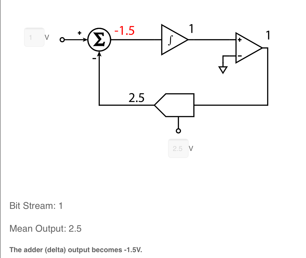
Here is a simulation of a 1 bit ADC with an integrator and comparators at input and output to determine the next bit to integrate to match the input with successive error integration and 1 bit ADC (comparator) of result relative to the reference voltage. This is how efficient high resolution, high speed Delta Sigma converters began. Then they evolved into higher levels of function with filters and serial interface logic.

\$\endgroup\$

Your Answer

By clicking “Post Your Answer”, you agree to our terms of service and acknowledge you have read our privacy policy.

Not the answer you're looking for? Browse other questions tagged or ask your own question.