2
\$\begingroup\$

If I take an advertised 50 ohm impedance cable and turn it into a coil will this change its characteristic impedance from 50 ohm to something else? My intuition tells me it should as if we look at one section of the coil the inductance per unit length should be higher as we still have the wires self inductance but the magnetic field produced now interacts with the neighbouring wires and induces a current in them which resists the initial current which sounds like the inductance per unit length would be higher which would increase the characteristic impedance. Is this correct?

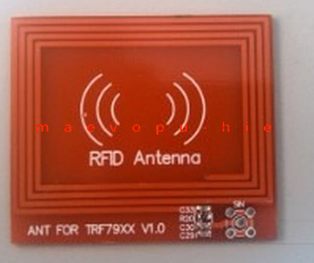
EDIT: For context I'm working on an RFID project which has an coil design similar to this enter image description here

Essentially I'm wondering if I set my trace impedance to 50 ohm and make this coil will the characteristic impedance of the trace be altered?

\$\endgroup\$
5
  • 2
    \$\begingroup\$ What kind of cable? Coax? Twisted pair? Twisted shielded pair (TSP)? Something else. \$\endgroup\$
    – SteveSh
    Commented Jan 25 at 2:16
  • 2
    \$\begingroup\$ How tight of a coiling? \$\endgroup\$ Commented Jan 25 at 2:20
  • \$\begingroup\$ In my case it's a PCB coil for RFID with a radius of 20mm and 4 turns. I asked this question as I'm assuming that if I set my trace impedance to 50 ohm but then coil it around itself this impedance will change. But I'd be interested to know if and how other cables are affected. \$\endgroup\$ Commented Jan 25 at 2:23
  • \$\begingroup\$ Do you mean a spiral pair of wires? \$\endgroup\$
    – user319836
    Commented Jan 25 at 3:16
  • \$\begingroup\$ I made an edit showing a coil design similar to the one I'm planning on making. \$\endgroup\$ Commented Jan 25 at 3:28

3 Answers 3

9
\$\begingroup\$

That's not a transmission line, that's a trace in space.

It would be a transmission line if the trace were over ground plane, and spaced adequately from nearby traces (microstrip geometry).

Follow standard calculation methods for square spiral inductors.


To explain in more detail:

A "normal transmission line", would be a well-defined pair of conductors, of constant cross-section, dielectric inbetween, and well-defined impedance and propagation velocity.

For the flat spiral geometry, you can think of (for very short time scales i.e. ≪1ns), one trace, with respect to its neighbor, as an edge-coupled flat (planar) differential pair; which will be a fairly high impedance, 100-200Ω say. But after the wave propagates once around the loop, now what was the signal becomes the ground, and vice versa.

The structure can't be modeled as a simple normal TL.

We further have the problem that, for each pair of traces, it's not against ground at all, but the companion of one pair, is in series with the next, and so on until the end of the winding. The transient impedance is actually a whole bunch of TLs in series (at the "start" port), then looped around in parallel (at the "finish" port, skewed by one index, except for the start and finish which connect to nothing else).

And furthermore, all the TL lengths vary, because the length around the spiral varies. (They're equal when it's e.g. a cylindrical helix, as in a single-layer solenoid coil.)

For more information along those lines, you might want to research the helical waveguide: this is one model of the helical solenoid winding, used to describe its impedance. The overall result is a much higher impedance (Zo in the kohms is easily achieved), and dispersion (propagation velocity varies with frequency). Similar analysis applies to the spiral case, with much stronger dispersion I suppose, and there are other known periodic structures with peculiar frequency response, meta-materials, etc.


Also consider the converse:

A transmission line is a transmission line, specifically because it is not an antenna. That is, EM fields are confined within the structure, rather than propagating out into free space.

Microstrip is a fairly poor example, as TLs go -- one whole side is open to space, and indeed radiation is noticeable from such structures. But it's usually low enough to be an acceptable compromise; for example, a 4-layer PCB with logic-level signals (e.g. LVCMOS at 3.3V and ~ns edge rate, or LVDS-style signals at ~10mA and ~Gbps data rates) can pass commercial emissions limits without much difficulty.

This is in direct contradiction to the purpose of an RFID coil: to couple to free fields.

A transmission line, as a trace over ground plane, is precisely the wrong thing to use here; the ground plane closes the loop local to the trace, greatly reducing the coupling to free fields. Rather, a loop antenna is normally used, with huge open area and no ground plane, specifically so that wireless communication is possible.

As above, we can still make some kinds of transmission-line-based observations -- but they become much more hand-wavey in nature, harder to scope out and model and analyze, and pretty quickly our one-dimensional analysis method (the transmission line) fails and we must submit to full-field 3D analysis.

Conversely, when we don't need the full-field analysis, as say at microwave frequencies -- it suffices to use low-frequency approximations. Hence the above suggestion to follow standard calculation methods. The most common of which I believe is due to Wheeler (sadly, often repeated but rarely cited!). Approximations by the way, that include ignoring various aspects such as wire shape, diameter, spacing, material (conductivity) and frequency; so expect some error (easily >10%) between calculation and the real article. This is worse than the tuning can be for an RFID gadget, so allow a step in the project plan to tune it -- for example, design for a low target value then increase load capacitance until on frequency; or iterate the layout until the self-resonant frequency is correct.


Finally, to answer the title question as curious readers may find it:

Does coiling a transmission line affect its characteristic impedance?

No, or not very much. If you wind up some coax on a spool for example, as long as the radius of curvature is much larger than the outer diameter, nothing much happens. Do observe that the cable is made of a range of materials -- the polyethylene or whatever dielectric is much less stiff and strong compared to the copper (or plated steel) conductors -- and so the cross-section becomes deformed when bent around, more and more as the radius of curvature approaches the outer diameter.

The resulting displacement, for tight bends or kinks, still doesn't amount to much for most signals -- it's a brief interruption where the impedance changes, and such changes are only sensible by waves by their size in relation to the wavelength. A deformation 1cm long is hardly sensible by a wavelength of 1m, etc. Such a kink can be detected by TDR (time domain reflectometry), where the wavefront length is comparable to the defect size.

Similarly, crushed cables can be detected by TDR; such is the basis of some traffic measurement systems for example.

The most important consequence from bending, is probably the reduced breakdown voltage, if the line is operated at high voltage (including at DC), or near the maximum [apparent] power rating. The core conductor being squished towards one side within the dielectric, causes the dielectric to thin, reducing its breakdown voltage. In the extreme, the core conductor can indeed get pulled all the way through the dielectric, shorting out the cable entirely.

Hence, you're advised not to bend such cables tightly. Always read the datasheet and supporting information from the manufacturer!
\$\endgroup\$
2
  • \$\begingroup\$ Thanks for the reply. I must have some flaw in my understanding. I thought any conductor can behave as a transmission line. Would a signal not propergate through the coil like a normal transmission line? \$\endgroup\$ Commented Jan 25 at 4:00
  • 1
    \$\begingroup\$ @SwissGnome We can approximate the electromagnetic behavior of an isolated single wire using a transmission line model. This is common practice in antenna theory, see kirkmcd.princeton.edu/examples/…. But it's tricky unless the radius of curvature of the wire is much larger than the width of the wire. \$\endgroup\$
    – John Doty
    Commented Jan 25 at 14:56
4
\$\begingroup\$

Not a transmission line

This is actually an antenna, or an air coupled coil. The aim of this structure is to maximize the transfer of energy through the air. Changing the shape of the coil will also change its characteristics.

Why 50ohms

If you design your antenna such it shows a 50ohm impedance to the circuit when coupled to the air, then you would have the most efficient emission and reception possible through that chain. This is called impedance matching and is required when dealing with RF signals. Of course, the impedance of the antenna will depend on the signal frequency, the PCB substrate used, the thickness of the traces etc...

Transmission line

The purpose of a Transmission Line is the exact opposite. It must contain the impact it has on the field within itself. It minimizes transmission of energy from the signal to the air and from the air to the signal by minimizing the distance between the signal and the return path. In the case of a flexible transmission line, as long as the coiling is not absurdly small in diameter, the impedance won't change that much because the current path stays more or less the same.

Some resources:

I can recommend this video from Zack Star. He explain most of this is a very nice way for an introduction. https://www.youtube.com/watch?v=pXWbdxOAuDs

\$\endgroup\$
3
\$\begingroup\$

As with most things in the world of electromagnetics, the answer is it depends. The characteristic impedance of a transmission line in a PCB is determined by several factors:

  • Dielectric material
  • Dielectric thickness
  • Copper thickness
  • Trace width
  • Trace spacing*

Many PCB CAD tools will calculate what trace width you need to achieve a certain impedance given the dielectric material, dielectric thickness, and copper thickness. For a two-layer board, these tools model your trace as a microstrip transmission line and perform basic calculations to determine the correct trace width.

enter image description here

Image credit: https://www.circuitbread.com/textbooks/electromagnetics-i/transmission-lines/microstrip-line (The bottom darker gray rectangle represents a reference (ground) plane on the PCB. The current needs a return path, and for a microstrip transmission line, that is a reference plane. The characteristic impedance is significantly impacted by the spatial relationship between the forward and return current paths, so it doesn't make much sense to think of a single wire as a transmission line. Although it may not be obvious in some cases, all antennas have a return current path.)

BUT

Your intuition is correct that if you have another trace get too close to your trace, you no longer have a microstrip transmission line, you have something else. How close is too close? That all depends on the self-inductance of the traces and their mutual inductance. The longer they run close together, the larger the mutual inductance, and the more effect they will have on their characteristic impedance.

Once you get too close, your transmission line is significantly different from a microstrip, and the basic microstrip equations don't apply. Your CAD tool probably will not recognize this or tell you about it. That is not always a bad thing. As you see with that RFID antenna image you posted, the trace is not spaced far enough apart to eliminate inductive coupling, but the designer likely changed other parameters to get the impedance, gain, frequency, and bandwidth they needed to meet their requirements.

If you're designing an antenna from scratch, I suggest a more sophisticated tool than your PCB CAD software, and an antenna design book. A common antenna design software is HFSS. There are books specifically about microstrip antenna design, although if you're still not entirely comfortable with the basics of transmission lines, you may want to start with an introduction to electromagnetics. I recommend "Fundamentals of Applied Electromagnetics" by Ulaby. It has a section on transmission lines that's very detailed but understandable if you are at least familiar with basic circuits. Good luck!

\$\endgroup\$

Your Answer

By clicking “Post Your Answer”, you agree to our terms of service and acknowledge you have read our privacy policy.

Not the answer you're looking for? Browse other questions tagged or ask your own question.