1
\$\begingroup\$

I am replicating one of our recommended designs for a POE application.

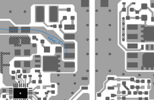
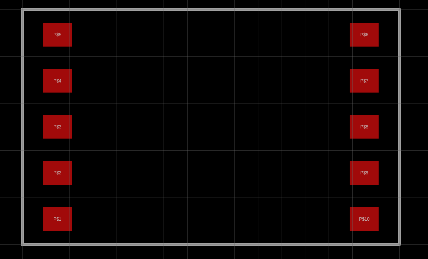
Here I have an EP13 forward transformer FCT1-50M22SL as recommended in the BOM. The pins do not match the provided image of the PCB layout provided. I understand pins 3 and 8 do not matter, but the component is not rotated.

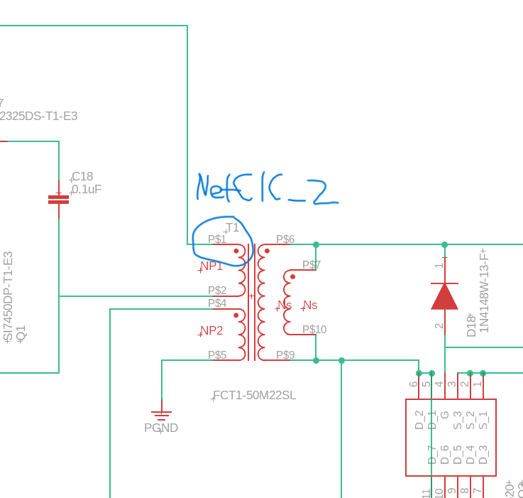
They are treating coil pin 1 as pad 2 & 3, pin 5 as pad 4, etc.

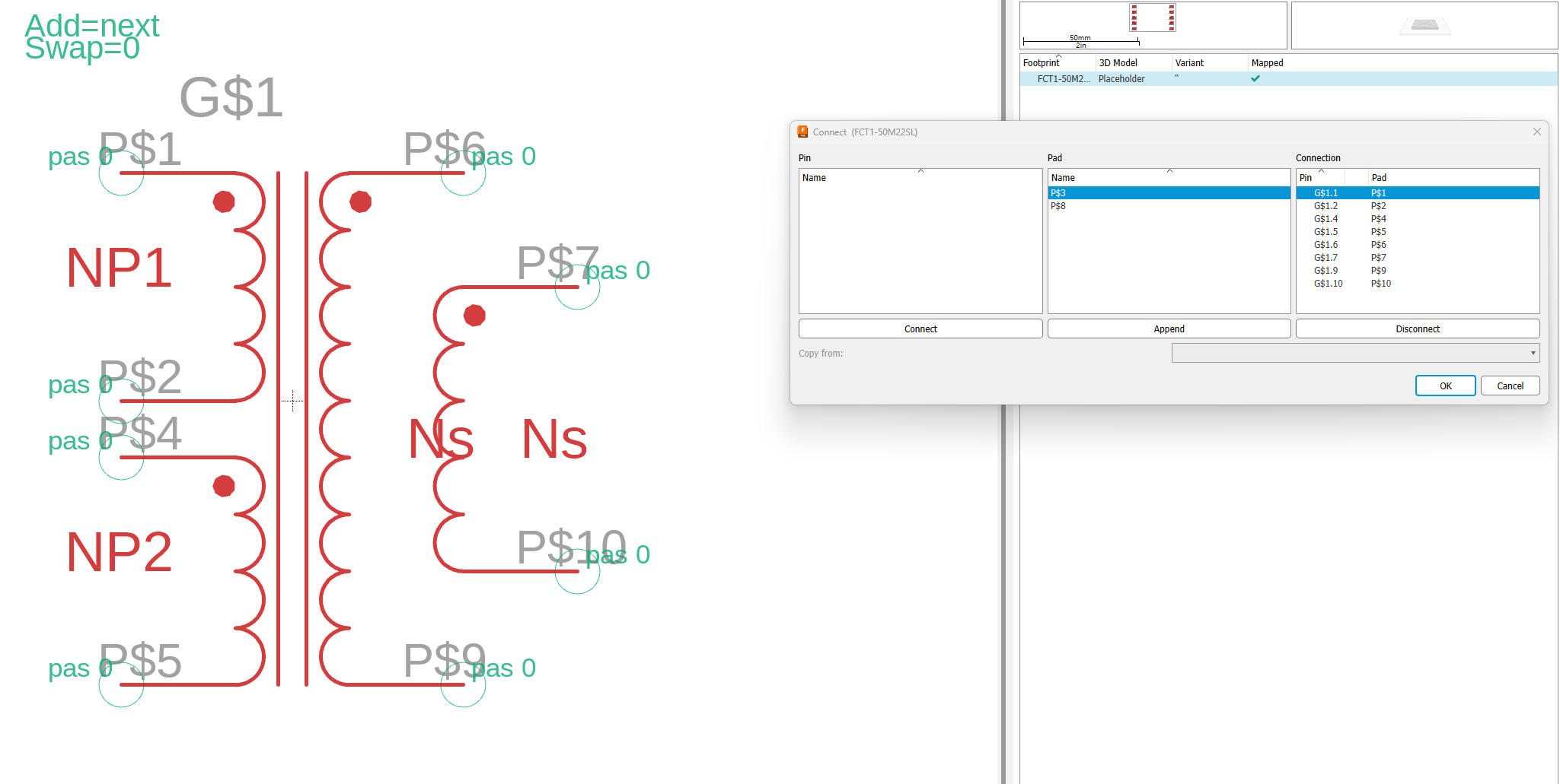
Am I wrong in thinking the model pins for the symbol are not pin 1 = pad 1? Are there other ways to configure the transformer and can I just use the image to map my pins?

enter image description here

enter image description here

Component I created from the reference

enter image description here

\$\endgroup\$
4
  • \$\begingroup\$ I do not see any discrepancy. Maybe if you described how you think the pins are it could be described what is noy properly understood. \$\endgroup\$
    – Justme
    Commented Feb 9 at 21:27
  • \$\begingroup\$ Yes, I changed the images to illustrate the issue where pad 4 is connecting in the recommended diagram to pin 1, where I expected that pour to connect to pad 1. Is there some way that I confused the component pins and pads? \$\endgroup\$ Commented Feb 9 at 21:36
  • \$\begingroup\$ Like I said, I can't figure out in which way you may have confused pins and pads. You need to explain it or draw it how you currently understand the pinout. \$\endgroup\$
    – Justme
    Commented Feb 9 at 21:46
  • \$\begingroup\$ One issue was the inverted pads, 1 should have been bottom left, etc. \$\endgroup\$ Commented Feb 9 at 21:59

1 Answer 1

2
\$\begingroup\$

I see two concerns:

  1. The given footprint is mirrored from convention. This is sneaky, because they give this drawing:
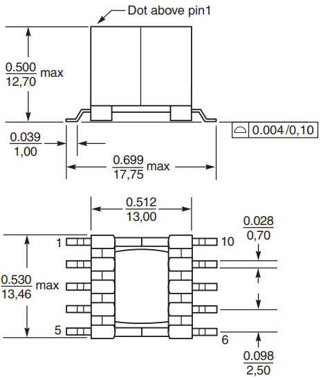
enter image description here

A cursory look might assume the pins are in the normal order, but the bottom drawing is the bottom view (hence the windings are visible inside the core). The land pattern is top-down, mirrored from this view.

You have a conventionally arranged footprint, which will swap primary and aux, causing poor and unexpected performance, or destruction.

In cases like this, I tend to ignore the numbering as given by the manufacturer, which is objectively wrong, and using a conventional pinout instead.

(It may be worth adding a note to this effect, to the schematic, or other design review materials, if other engineers will be looking at this and double-checking your work.)

In that case, you should change the schematic to have bias on pins 1-2, primary 4-5, and the secondary is in the same place, give or take phasing.

  1. You can swap all windings end for end, to get the same response; at least at low frequencies.

At high frequencies, it may be preferred to keep one or another end of a winding near GND, or referenced to certain ends of other windings (typically VCC and GND, both being AC-ground nodes), and then the choice of which end to ground matters, or which end of the winding the rectifier diode goes on. (With a sync rect, I think this probably isn't applicable here, but to say there are cases when it is.)

For such a small transformer, and at low to moderate voltages, this probably doesn't make a difference. It may also be that the transformer isn't made with the particular winding techniques, or shielding, where this would affect the result (in other words: don't worry about it).

It's also a "don't worry" situation if you won't be re-doing the design, to optimize transformer windup, component placement, EMI filtering, etc. Since, you'll do the design, the EMI filtering is whatever it needs to be, and that's that; maybe it could be simpler if a more suitable transformer wiring or windup were chosen, but if these aren't variables you're going to test, then the EMI is just whatever you get with the configuration you will test.

Assuming of course, that EMI is a concern and will be tested.

\$\endgroup\$
4
  • \$\begingroup\$ With the corrected Footprint, I should just change the schematic to use 1-2 for bias, and 4-5 for primary, correct? Thanks by the way. \$\endgroup\$ Commented Feb 9 at 22:04
  • \$\begingroup\$ Ahh, now I can just reverse the connection on pin 1-2 and it matches the pcb layout. Is that fine, To reverse winding pin connections? \$\endgroup\$ Commented Feb 9 at 22:06
  • 1
    \$\begingroup\$ Yes. And when you swap pins 1-2, also swap 4-5, and 6,7-9,10. I can't see the rest of the circuit but I expect that is what they had done. \$\endgroup\$ Commented Feb 9 at 22:11
  • \$\begingroup\$ Yes, I can tell from the pcb layout and pinout that you are correct. So reversing the pins reverses the polarity of the transformer? I guess they must have done this in their component, as that would be the only way to match up the schematic to board. \$\endgroup\$ Commented Feb 9 at 22:16

Your Answer

By clicking “Post Your Answer”, you agree to our terms of service and acknowledge you have read our privacy policy.

Not the answer you're looking for? Browse other questions tagged or ask your own question.