This question is really asking two:
What is the best way to wake from sleep with the press of a button?
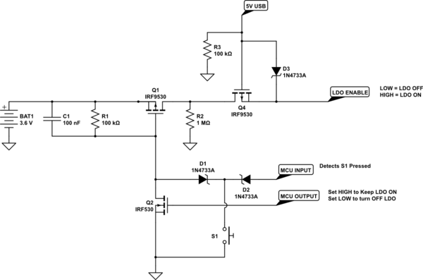
What is the best way to combine power sources such that the battery is not charged by the USB source? (why do you want that behavior?)
Part 1. "Digital" wake from button press
This is a low Iq design approach (ha ha)
You are trying to implement a low power (a.k.a. "deep sleep") shutdown condition with digital restart. The broad class of engineering research describes this scenario as low Iq design... "I" = current, "q" = quiescent (latin for "resting").

The Problem(s)
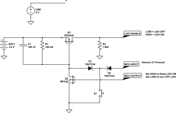
The question's proposed design uses an approach known as "suicidal hardware" (a controller that can kill its own power supply), which is generally a bad idea fraught with all kinds of stability and "brick-ing" problems.
For example, what happens when static, environmental, radiated, or triboelectric charges appear on the control line to the power supply? The state of the high-impedance output will change and change erratically resulting in the power supply cycling, greying-out, or de/activating unintentionally. To combat this you can add bias resistors, but these will add a permanent quiescent current drain.
Similarly, what happens if you have a programming error (during development or, later, during a patch/update of the firmware) that doesn't sequence the power supply control pin correctly? It's then possible that the MCU starts up, turns it's power supply off, the presence of the USB charger causes it to power up again, then the MCU turns it's power supply off, etc, etc... this loop occurs so quickly as to make intercepting the startup sequence with test equipment (JTAG devices, ISP devices, et al.) very difficult. Again, you can add hardware to deal with this, but all of these devices add to the static quiescent drain.
You also need to explore the entire body of design literature around power domains because if your LDO floats its output during shutdown (enable asserted low) the MCU's internal electrostatic discharge protection is partially compromised.
There are other scenarios beyond my attention span to describe here... I think the point is sufficiently illustrated.
The Answer(s)
The scenario you've described is VERY common in battery powered devices with accessible wall chargers (think the most widely mass produced consumer electronic device category in human history -- CELL PHONES).
If you want your microcontroller to wake on button press (and usually to do different things based on how the button is pressed -- long press = recovery mode, short-press = deep-sleep, clicked = sleep, et al.) there is no alternative than to keep some kind of controller/logic-circuit "awake" in its lowest power state. To support that you need a power supply that also has a low-Iq deep-sleep supporting mode.
Until about the last few years (in which cell phones became so mature as to have all of the logic and power supply of the phone integrated into single chips), Cell phones would have (generally) two processors and two power supplies: (1) The main application processor (and the associated high power capacity supply to drive it) and (2) a very lower operating and quiescent power microcontroller to handle all the deep-sleep states (and state-transitions).
Your design baseline
To understand why your intuitive approach of "MCU just disconnects its own power supply to save power" doesn't work well in practice, we need to examine it's actual quiescent draw in its "deep sleep" (e.g. "off") state.
Note: Power FET's are notoriously leaky, so you could address some of these issues, just by choosing parts that are sized and typed more optimally for your application.
You've selected the IRF530 family of NFET/PFET which have the following leakage characteristics (IRF530 shown; the IRF9530 is the same leakage, just the opposite direction).
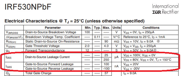
There are (at least) 3 main leakage discharge paths from the battery when the MCU has turned off its power supply:
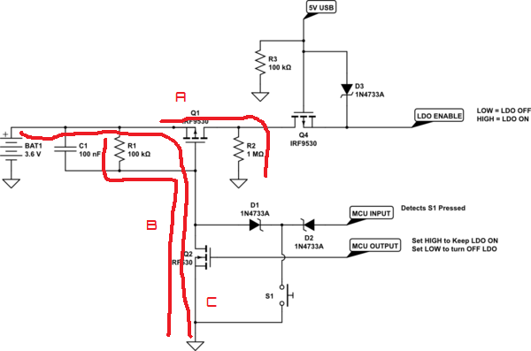
[A]
The battery --> backwards through Q1 --> through R2
Q1 will leak up to 250 microamps, but the leakage will be limited by R2 to approximately 3 microamps.
[B]
The battery --> through R1 --> backwards through Q2
Q2 will leak up to 250 microamps, but the leakage will be limited by R1 to approximately 40 microamps.
[C]
The battery --> backwards through Q1 --> backwards through Q2
Q2 will leak up to 250 microamps, but Q1 will limit the leakage to 0.1 microamps
[D]
The battery --> LDO
The LDO even when the enable signal is asserted low (e.g. disabled) still has a quiescent (leakage) current.
[A] + [B] + [C] + [D] > 43uA (ish)
Your "best" case power consumption when completely "off" will not actually be that low by low-power (e.g. low-Iq) design standards.
A Better Approach
1. Don't bother with LDO shutdown
An LDO -- really, an LDO-LVR -- is a Low Drop Out Linear Voltage Regulator. The "linear" part is the most interesting here. Linear voltage regulation means that the power lost in the regulation process is linear with the power demanded by the load. This is great news because when the load is "sleeping" the power supply will automatically sleep with you.
As example, this is the Microchip MCP1700T:
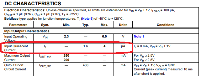
It's nominally just 1.6 microamps -- far below the leakage of your switching components. That is, for all the work you're doing in the design and assuming you could use literally perfectly performing components, AT BEST you're only going to remove an additional 1.6 microamps (about 7 microwatts) from the design. In practice, you can't achieve this.
2. Use the MCU's existing dedicated hardware
The question doesn't state which MCU you are using, but even if you are using a pretty powerful/capable ASIC like an ESP32. Using firmware which takes advantage of hardware the ASIC designers already included for deep-sleep and low-power applications, you can achieve a quiescent power of around 150 microamps... while still retaining the ability to wake by radio! If you want to only wake by button press, you can get below 50 microamps on this platform.
If you're deep-sleep performance is the critical design parameter, there are MCU's that can sleep in the nano-amp regime -- which is practically 0 as leakage within the surrounding system will be at least an order of magnitude greater.
Conclusion: Use firmware
So in summary, all this extra hardware added to the design to manage the power state is only hurting the design in terms of power, complexity, cost, and design time.
This is a common and solved problem. The parts you are using already include the hardware you need. Just take advantage of it! =)
Part 2. Combining voltage sources
You can do this many ways, but the most practical is through the use of a Load Switch.
Load Switches
Load switches are PFET's (typically) packaged with all of the supporting hardware needed to make them practical and protected. Texas Instruments provides a brief overview video here:
https://www.ti.com/video/5412304837001
Example Design
In your case, here's an example design using TI's LM66100. Many other manufacturers make load switches and you should choose one that is sized for your application to minimize the parasitic effects the load switch will have on your quiescent power and material cost of your manufacturing.
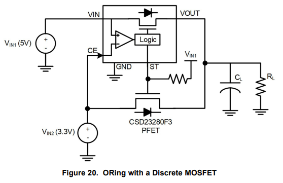
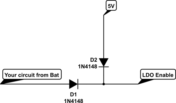
This configuration uses two load switches to create an "ideal diode" OR-ing network -- the behavior of a two diode network, but without the voltage drop and inefficiencies of using actual diodes.
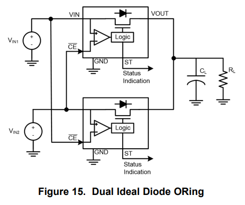
This is an alternate configuration that uses the Status Output pin of the LM66100 to control a discrete P-Channel MOSFET. This can be useful in applications that want to minimize the leakage current on the secondary supply (your battery), at the expense of more leakage on the primary (USB). This configuration can also be used on systems that require a lower R_ON on the secondary (battery) path, useful for higher current applications or applications sensitive to noise or high frequency stability.
Part 3. Conclusion's conclusion
Even if you aren't planning for a custom PCB or any kind of production, you can achieve better performance and all of your desired features simply by removing your proposed circuitry, updating your MCU firmware, and "OR-ing" your power sources (battery and USB) with load switches. Load switches are even available in easy to hand-solder/prototype DIP packages.
Best of luck with your project!


LDO ENABLEa logic signal only or a power input to your LDO (or the rest of your circuit) as well? \$\endgroup\$LDO ENABLEis a signal only connected to the enable pin of the LDO. LDOVinis powered separately. \$\endgroup\$