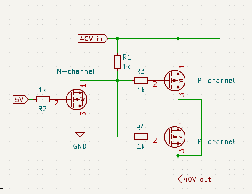
I would like get some feedback on the given subject. I want to control the N-channel MOSFET using a microcontroller and use 2xP-channel MOSFETs to increase the current capability. What I'm doing as you can see from the schematic. I'm pulling the gates of the P-channels up to the main voltage using a 1 kΩ resistor to reduce the current. This works nicely with a single N-MOSFET and a single P-MOSFET. I'm a bit puzzled when the second P-MOSFET is added to the circuit. Do you guys think there is a need for R3, R4 or it can work without it? Thank you
-
3\$\begingroup\$ I'd rather worry -40 V may be way over \$V_{GS_{max}}\text{ }\$ and check with the specs. Increase R3&R4 to 1K8 and use 470 Ω from each gate to source to limit \$V_{GS}\$ to about 9 V. \$\endgroup\$– greybeardCommented Jun 30 at 13:43
-
4\$\begingroup\$ (Um - wait - aren't S&D swapped with the P-channel FETs?) \$\endgroup\$– greybeardCommented Jun 30 at 13:45
-
\$\begingroup\$ The PMOS transistors are upside down. At the moment the body diode is always conducting. SG-voltage reaches 40V which is to much for most transistors. At DC R3/R4 are not really needed. Instead put small resistors in series with each source. \$\endgroup\$– RaonokeCommented Jun 30 at 17:42
-
\$\begingroup\$ @greybeard thank you very much I actually used it before but it was all up to 12V so never thought about Vgs about the pMosfet. Created this simulation according to your recommendation but with only a single pmosfet. does this look right? (nevermind that 100 ohm resistor at the bottom thats just a load placeholder) tinyurl.com/2p96a66q \$\endgroup\$– OrnitelCommented Jun 30 at 18:52
-
\$\begingroup\$ @greybeard and this is with the dual p-mosfets tinyurl.com/2h9hqaho \$\endgroup\$– OrnitelCommented Jun 30 at 18:59
2 Answers
If you ask about R3 and R4, so the main topic is gate resistor.
In your schematic, R1 just being a current current reducer, so R3 and R4 will be essentials depends on your design.
Edit: it will work without R3 and R4.
More about gate resistor and why you should use it: https://www.youtube.com/watch?v=fsgKpAq2gd0
-
\$\begingroup\$ Thank you for the answer, after the post i created the example in circuitjs for simulation and indeed it works. In this case i will probably omit the R3 and R4. I will definitely watch the video. \$\endgroup\$– OrnitelCommented Jun 30 at 13:34
-
Unless you are driving the FETs at a high switching frequency, or the circuit is in an application that is sensitive to very short, very small VHF noise bursts, R3 and R4 are not needed.
At first glance, it appears that R1 is much smaller than it needs to be. This leads to excessive power dissipation; 1.6 W in your case, requiring a 3 W part for good long-term reliability. Increasing it to 10 K looks fine, but it can affect the output.
Depending on the actual part numbers for the two output FETs (reference designators - !), their gate capacitances can be significant. For example, if each FET has an input capacitance of 1 nF, the time constant of waveform the gates would see is 2 us with R1 equal to 1 K, and 20 us with R1 equal to 10K. We don't know anything about the input or output waveform requirements, so only you can say if this is significant.
There is nothing in the circuit to assure balanced current sharing between the output FETs. FETs are better than bipolar transistors at self-balancing, but adding a ballast resistor in series with each source gives you more control over this. However, it also increases the circuit's output impedance, as well as the overall circuit power dissipation.
Now, for the real problem . . .
The FETs are either incorrect parts or connected incorrectly, depending on your design intent.
You show the FETs as source-followers, not saturated switches. If this is what you want, or need due to signal logic polarities, then change the FETs to n-channel types. A source-follower can act as a switch, but it is non-saturated. Thus, the voltage across them always will always be greater than their rated threshold voltage, significantly increasing their power dissipation. There is a simple circuit change that can reduce this dramatically, if you can invert the logic polarity of the input signal.
Also, as pointed out, the internal body diodes are a problem. If you reverse the source and drain connections, then the FETs act as saturated switches and the circuit needs one additional resistor (R4). R1 and R4 form a voltage divider to assure that the "gate voltage" (actually, the gate-source voltage Vgs) does not exceed the max rating for the part. For many power MOSFETs this is 20 V, with 10 V needed for maximum enhancement (complete turn-on). One way to achieve this is to leave R1 at 1 K and add in R4 at 2.2 K to 2.7 K. Again, scaling these values up by 10x reduces power dissipation and component size.
-
\$\begingroup\$ Thank you for the detailed response. As others previously indicated seems like the SG voltage for pMosfets can get to 40V which is not acceptable as the datasheet indicates it can be +-20V. This is something i overlooked and to be honest never thought about it because i always worked with 12V max until now. So here is the updated version of the schematic, i think it looks ok but as per your recommendation i will increase that 470ohm and 1.8k to a higher values and i guess that should be good. tinyurl.com/2h9hqaho \$\endgroup\$– OrnitelCommented Jul 1 at 14:09
-
\$\begingroup\$ What is the actual peak load current? \$\endgroup\$ Commented Jul 1 at 19:48

