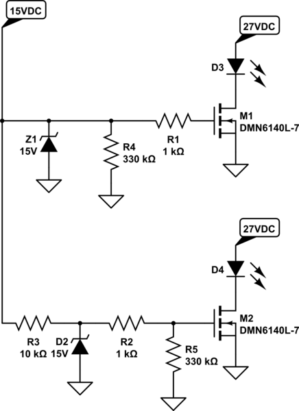
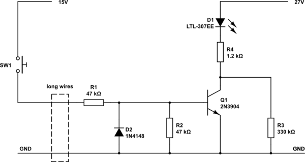
There are two main situations as I see it here, and two additional circumstances that are mostly/completely undefined yet reasonably suspect.
Situations
Handling ESD
For a part not in circuit, this falls under the Charged Device Model (CDM) test, such as published in ANSI/ESDA/JEDEC joint standard JS-002. Capacitance and energy are small, but risetime is fast.
Typical scenarios relate to handling parts in their packaging: this may include partial discharge across charged surfaces of non-dissipative packaging (that staticy sound you get when rubbing plastic; discharge can occur near/around (induced ESD) and through (direct strike) the device in question), or charge due to handling or removing the part from its packaging (triboelecticity), that isn't dissipated due to it not being in contact with said packaging anymore (e.g., dumping parts out of a tape or bag, bouncing on the table, etc.).
HBM (Human Body Model) is also likely (touching, moving, placing, etc. parts), hopefully at lower voltages. Where ESD controls are in place (say, using a grounded table, dissipative mat, and wrist strap), voltages under 300V are typical, which most parts are rated for.
ESD is a typical datasheet parameter, so we are done here: it's specified directly.
Wired ESD
For a part in circuit, we test the system to IEC 61000-4-2, at various levels as needed, or to other standards as applicable (automotive applications might use ISO 10605, etc.). Typical commercial equipment is tested at 6/8 or 8/15 kV (contact / air discharge). The pulse waveform has a rapid rise (contact discharge, couple ns; air discharge, ~10ns), and a duration of 50ns or so (50%-50%).
To a second order approximation, the equivalent circuit of an ESD generator is an RLC series circuit. The capacitor is charged to some initial voltage (the nominal rating of the test), and the circuit is closed onto the EUT (or nearby objects and surfaces: coupling planes, capacitive clamps, connectors, etc.) via a high-voltage switch (contact discharge) or air spark (air discharge). The RLC circuit defines a peak current \$I_{pk} \le \frac{V_{pk}}{Z_o}\$ where \$Z_o = \sqrt{\frac{L}{C}}\$, and also \$I_{pk} \le \frac{V_{pk}}{R}\$ (because both inductance and resistance act together to increase the loop impedance). Typically R = 330Ω, so a 8kV test can deliver 24A peak.
As the ESD pulse travels, it inevitably dissipates. This is truly a light-speed phenomenon, with such short risetimes in question. An ESD strike to a wire, has it radiating away high-frequency components, inducing charge or current in nearby elements. A strike to a plane, spreads it out in both directions, as the energy propagates along and around the plane. The capacitance from plane to EUT can couple significant energy in, and in unexpected routes -- truly, the EUT is bathed in an electromagnetic pulse (EMP), and if energy can find a way in, it will.
At greater distances through space (say, several m), the severity of the pulse is greatly reduced. Even conducted along cables, it's likely to round off (slower risetime) and attenuate, and after some 10s of m, it may no longer look like ESD anymore. (Mainly due to the dispersive effect of real cabling installations: cable trays, raceways, etc., or branching circuits like mains wiring; and the high-frequency absorption of common jacket and insulation materials, like PVC.) Energy is also dissipated in the sense of, being spread out into other modes: the waveform may pick up various squiggles as different cables and structures in the environment resonate from the strike; this has the general effect of softening the peaks; basically, more voltage and charge is distributed over more surfaces, with more oscillation at more frequencies, and peaks at any given location are diluted as a result. (Though sometimes, the "perfect storm" of reflections comes together and makes peak voltage/current even worse at some particular point in the system -- potentially even at some distance from the ESD gun itself. Not saying it's likely, just saying it's possible. For a contrived example, consider a pair of parabolic reflectors, with the ESD gun at one focus.)
For a situation like yours, a strike to either cable, or a strike to metal nearby either cable route, will introduce significant energy to the section of the circuit in question.
For the MOSFET, we need to know what voltage and current are imposed on it.
A direct ESD strike, from ESD gun, into one terminal, out the other to ground -- a very simple system, no wiring at all -- can only be dealt with by shorting out the pulse (or by withstanding its full voltage -- but we can discount that possibility for essentially all discrete semiconductors :) ), and enduring the peak current for the pulse duration.
For D-S or S-D strikes, many parameters are relevant: maximum or breakdown voltage, maximum (pulsed) current, rate of rise (dV/dt), drain capacitance (Coss), and maximum gate voltage and D-G (Crss) and G-S (Ciss - Crss) capacitances. Violating any one of these ratings, whether directly, or by way of the capacitance dividers implied by the parameters, and device failure is expected.
Note that MOSFET capacitances vary wildly with terminal voltage, in particular with VDS. The tabulated values are irrelevant here: we must model the effect of the ESD pulse upon the device, causing voltages to rise, capacitances to fall, voltage rises faster, etc. etc. This is easiest done by preparing a representative model of device capacitance (say in SPICE) and connecting it to a pulse generator.
For a direct G-S (or G-D) strike, mostly gate capacitance and spreading resistance are implicated. The spreading resistance is rated as a lumped equivalent, but it's due to the distributed resistance between MOS cells on the actual chip. Therefore, the voltage drop across it is relevant. Even large power MOSFETs with a few ohms RG, this parameter is relevant: 24A peak * 2Ω = 48V, well over the VGS rating (which might be 20 or 30V; actual breakdown might occur anywhere from 30 to 100V -- you never really know until the instant it blows through). Even without resistance, gate capacitance must be truly massive to have significant effect against ESD: ignore the R and L in the ESD generator equivalent circuit for a moment and consider the capacitive divider, between the say 150pF at 8kV, and a CGS at 0V initially but rising to no more than say 30V. To have such an outcome, CGS > 40nF. That's a big chip. Such devices do exist -- but keep in mind, considering the above, it'll have to be even bigger (perhaps 100nF or more) to have a good chance at withstanding a direct hit, when including the effect of resistance.
A marginal capacitance also can't withstand two or more direct strikes, which would continue to charge it up.
It is for this reason, by the way, that power supplies are generally ESD safe, as a direct target, or by way of clamping diodes (at least, in the differential mode; mind that there can always be extenuating circumstances that take priority). With a few µF shunting the supply, and a short distance from any strike target to bypass capacitors, the transient overvoltage can be quite modest (a few V). For low-power circuits, a clamp diode (TVS) may still be desirable to discharge any excess, as it could still get overcharged by repeated strikes; but most stuff that isn't minding its power consumption will have no problem from that.
But we also aren't asking about a bare MOSFET. There is more to consider:
Circumstances
Is the wired ESD due to strikes on or near the cable?
Direct strikes, conducted, we can expect fairly large currents crossing the circuit.
The equivalent circuit of cables through space, has the pulse imposed on their characteristic impedance (a cable loosely over / near a ground plane, likely has an impedance from 50 to 150Ω; in free space, maybe 200 or more, or the concept of characteristic impedance starts to lose meaning by then), and propagating up and down the cable from the strike point. This provides some voltage division, and perhaps a 8kV strike is reduced to 2-3kV on the cable.
As discussed above, the risetime may slow, or ringing is introduced, depending on losses in the cable, what it's routed near, etc.
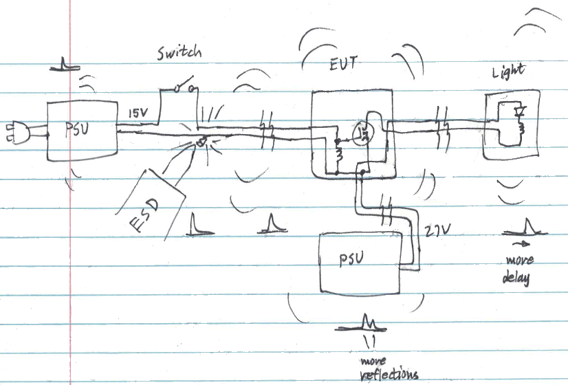
In transient terms, from any point on a cable, looking left and right, there's a source impedance of Zo, going into a load impedance of Zo; so we expect peak voltage and current on par with this (i.e., a few kV and maybe 8-15A). Note this propagates in the common mode, around outer shield if applicable, or shared among conductors if not. We might have a situation like so:

Suppose some part of the circuit is struck with ESD. The pulse almost instantaneously raises the voltage on direct and nearby wiring, and propagates outward from it. The whole system becomes energized in turn, at some point in time; the pulse waveforms shown at various points suggest the time delay along cabling, as well as possible reflections picked up from various ends (whether reflecting off bulky units like PSUs or actual ground points, or open circuits like the far end of the LED cable, perhaps).
Notice that we have similar situations for induced ESD, i.e. striking a nearby object, to which the cable has some capacitive coupling, or characteristic impedance. The pulse has a differentiated waveform, with positive and negative peaks, but the impedance is still determined by cabling and the amplitude isn't much lower (depending of course on how well coupled the objects are).
Don't overlook the effect of the switch itself. Mechanical contacts close in a fraction of a nanosecond; this launches a wave down the 15V cable, in both directions, and when it whips off the far end (your R3) the voltage doubles up to 30V peak. (This can be even worse with nonlinear capacitors, as is particularly common in power supplies.) If this were direct wired to the gate, destruction would be likely, even in the complete absence of ESD.
Is the wired ESD damage due to poor layout?
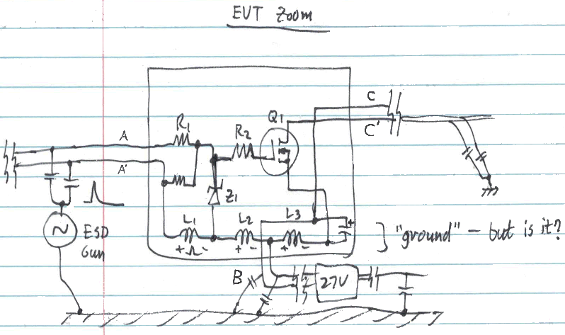
Consider the EUT section in detail. There are wires entering and exiting the area:

Note that ESD manifests as a (direct or capacitor-coupled) transient, into any wires of the cable. As mentioned: the outer shield if applicable, otherwise most wires within (as shown). This can be considered a Thevenin source with respect to some ideal reference plane (ground hashing in the diagram), but notice you do not, in general, have any connection to that reference plane in your actual circuit: your circuit is distant from it, and at these time scales, pure distance alone is sufficient to violate our usual assumptions of ideal grounding.
Cables themselves have distributed capacitance to ground (or other surroundings), as shown at B, on the right, etc.
Now consider the in-circuit ground. If this is made with a solid plane (and some other considerations to component placement), we can expect very low inductance along it, and the AC/transient voltage drop from A' to B to C can be very low (as seen from within the circuit). Thus we can treat ESD entirely as differential mode, with respect to this circuit reference plane, and are only concerned with what wires A and C' are doing.
If ground is made poorly (point-to-point wiring, large loops, etc.), inductors L1-L3 are significant compared to the amplitude and risetime of the pulse, and drop significant voltage (10s, 100s V even). Remember, the risetime is short, a few ns, so along the length of a cable, voltage rises from 0V to a few kV over maybe a meter (or less!). If the zener diode is connected as shown (midway between ground points), considerable voltage can drop in the loop with it and the MOSFET, destroying it. Notice this applies even if wire A is disconnected!
Keeping the gate loop short (Z1, R2, Q1) is paramount for Q1 survival. A TVS on C' may also be desirable, for the same reason (when Q1's drain/channel isn't suitably rated for ESD strike).
Best Practices
To summarize:
- Keep ground paths short, and priority loops small. Priorities around a MOSFET switch are G-S and D-S circuits.
- Use ground plane layout techniques. Avoid coupling from loose wires or traces, into critical sections of the circuit.
- Use resistance to dampen ringing and increase cable/ESD impedance.
- Use TVS or clamp diodes (where applicable) to shunt ESD around sensitive circuits/elements.
- Use filtering to slow risetime, and provide radio-frequency (RFI) immunity.
