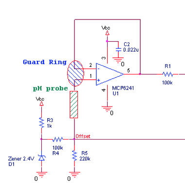
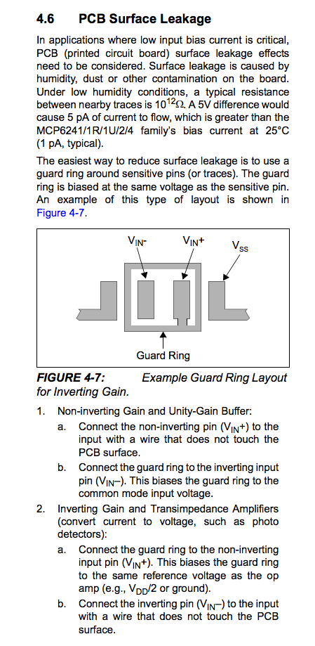
A guard ring is supposed to be at the same electrical potential as the input it is guarding. This reduces leakage from that node. In its simplest form it is just a same-potential ring around the sensitive node, but it can also be a driven ring and/or trace via a separate unity gain buffer.
The purpose is to not have any voltage difference (or at least to minimize it) from the protected net or node to anywhere else, and thus no path for leakage.
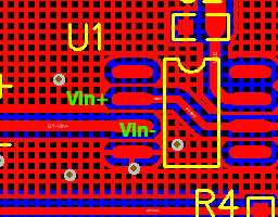
Using a ground plane as a guard ring is downright stupid and clearly shows that your PCB designer doesn't know what he is doing, as the ground plane is the exact thing you don't want near the sensitive node. When I am designing a PCB with guarded nodes, I often cut-out and pull back any planes under the sensitive node(s) and also pull back the solder mask too. You want nothing there but the guard ring.
Furthermore, you need to consider the trace to the guarded pin as well. Which, by the way, you have backwards on your screen-capture of the PCB ... The trace entering from the left on your diagram is from the sensor and is going to the Vin+ pin, not Vin- as you have indicated. The Vin- should wrap around Vin+. That long input trace coming from the left side should be guarded as well, or come up with a way that gets the input signal to the Vin+ pin without going across the board like that. At the very least, the ground plane around that trace should be pulled back considerably.


