1
\$\begingroup\$

I'd like to ask for some advice on the circuit described below:
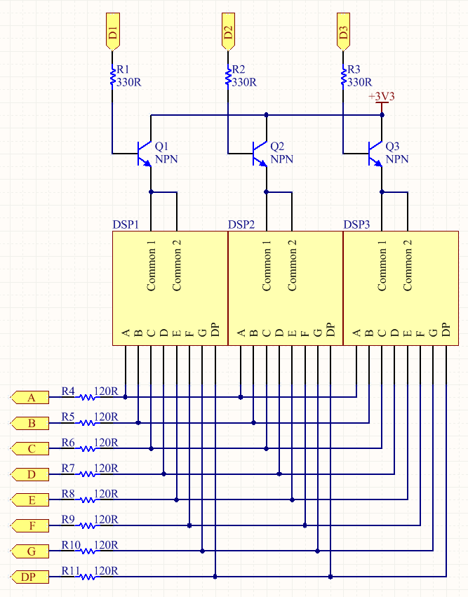
enter image description here

I'm building a matrix of multiplexed seven segment displays, with common anode. The ports D1-D3 and segments A-DP will be driven by I/O pins from an LPC1114 ARM microcontroller.

As I understand the datasheet specs for this part I cannot exceed 4mA of source or sink current in the standard purpose I/Os. See this question for more clearance on this.

The display datasheet says that the forward voltage of each segment of the display is about 2.10V. They will be feed with 3.3V. I want use 10mA of current in each segment (I believe it will give a nice brightness with this current).

With all this in mind, and for what I understand of electronics, I aks these questions:

1 - I cannot connect the segments A-DP directly to I/O ports since it will exceed the sink capabilities of the I/O. Is this correct?

2 - Almost all schematics I found on the web on multiplexed displays do that. I did not found anyone that deals with this problem. What suggestions do you have to make it possible to sink more current in each display segment?

3 - I thought that maybe I could sink segments A-DP to ground using a MOSFET controlled by I/Os. Is this a good idea? What do you think? Any schematics on this?

Thanks

\$\endgroup\$
2
  • \$\begingroup\$ There are 7 segment drivers designed for this exact task. \$\endgroup\$
    – Matt Young
    Commented Jun 10, 2014 at 14:17
  • \$\begingroup\$ Or you can use shift register ICs (4014 or 4015) \$\endgroup\$
    – Alexey
    Commented Jun 10, 2014 at 14:34

3 Answers 3

5
\$\begingroup\$

1) Yes that's correct. If your GPIOs can source or sink 4mA you can't ask them to source or sink more, they probably are overcurrent protected but they won't work properly.

2) That may be because other designs use "stiffer" GPIOs that can source/sink all the current that is needed.

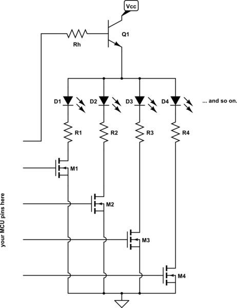
3) That is a great idea. You can use a mosfet or a transistor, just like you do on the high side. Why are you using a NPN bjt for the high side anyway? A p-mos or a PNP bjt would be better in my opinion.

The schematic is simple:

schematic

simulate this circuit – Schematic created using CircuitLab

Remember that when sizing the limiting resistor you should take into account Q1 saturation voltage and Mx on resistance (that's quite low actually).

Pay attention to maximum mosfet \$V_{GS}\$, 5V might be too much, and be sure that Q1 is fully saturated also when every segment is on, i.e. when its collector current 80mA. Of course its collector current rating must be high enough.

As I said you should probably use a p-mos for the high side switching, currents are low so you can find something suitable for your application. Please note that a NPN bjt might not be suitable since the micro controller output is lower than 3.3V, then you have a \$V_\gamma\$, that's another 0.7V, then the LED, then the N-MOS... If the micro output is too low your leds might not light at all.

\$\endgroup\$
1
\$\begingroup\$

You can use a bunch of NPN transistors that act as pull-downs on the 8 common lines feeding the displays. You'll still need a resistor in series with each of course. Your anode voltage is going to be about 2.7 volts (emitter follower loses ~0.6 volts) and assuming your LED drops 2 volts when being powered at 10mA, this leaves a resistor value of 0.7/0.01 = 70 ohms.

If you used PNP transistors on the high side, you'd probably only lose about 0.1 volts up there leaving 3.2 volts on the anode and about 1.2 volts on each current limiting resistor. This makes the resistance 1.2/0.1 = 120 ohms (as you have shown).

Obviously if you use 8 more transistors you don't exceed the IO spec but there is an inversion in logic to fix. Ditto if you swap to a PNP transistor as common emitter on the anodes.

\$\endgroup\$
0
\$\begingroup\$

This could be a more difficult question than it first appears, especially if you're planning on driving a blue or white LED display. The forward voltage of those can approach the 3.3V you have available, so you cannot afford the ~0.9V voltage drop of your NPN emitter-follower transistors (you could lose the 330R resistors in that configuration, by the way).

You could use low voltage P-channel MOSFETs for digit drivers) and N-channel low-voltage MOSFETs to drive the segments.

For example: N-channel FDY3000NZ (dual MOSFET) for segment drivers common anode P-channel AO3415 (single MOSFET) for digit driver common anode

That combination will result in a total voltage drop of less than 100mV at reasonable currents for a 3-digit display, meaning most of the voltage will end up across the LED (making light) and the resistor (equalizing the light between segments).

I suggest gate resistors on all MOSFETs (1K should be fine for sensible multiplex rates) to control the current flowing from the outputs to the gates. You may have to blank briefly between digits to prevent ghosting.

\$\endgroup\$

Your Answer

By clicking “Post Your Answer”, you agree to our terms of service and acknowledge you have read our privacy policy.

Not the answer you're looking for? Browse other questions tagged or ask your own question.