3
\$\begingroup\$

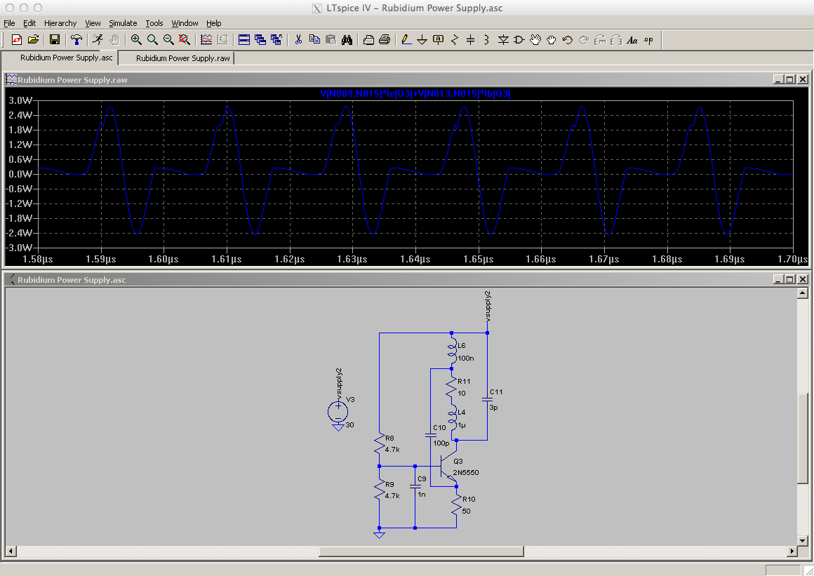
I'm using LTSpice to model a LC oscillator, driven by a NPN transistor. When I used the power calculating function on the transistor, LTSpice indicated that during part of the cycle the power dissipated in the transistor is negative. I was under the impression that transistors always dissipate power resistively since they don't store energy in E or B fields.

So my question is, what am I to make of this? Should I take the absolute value or something?

EDIT: As requested, here's the asc file: http://pastebin.com/F1wBPXVy

Pic showing the transistor power in LTSpice.

\$\endgroup\$
10
  • 2
    \$\begingroup\$ Since you have it available, it would be most convenient for people trying to see for themselves to provide the .asc file. Anyways have a look at the transistor connectors in which direction current is flowing tehre. \$\endgroup\$
    – PlasmaHH
    Commented Jan 15, 2015 at 16:38
  • \$\begingroup\$ Not that the asc format is just text, so pastebin.com and similar work well enough for uploading that. \$\endgroup\$ Commented Jan 15, 2015 at 16:49
  • 1
    \$\begingroup\$ @RespawnedFluff: right click, open in new tab. its a 2n5550. Btw. I am pretty sure he exceeds the emitter base voltage. \$\endgroup\$
    – PlasmaHH
    Commented Jan 15, 2015 at 16:56
  • 1
    \$\begingroup\$ Yeah, this is a 2n5550. And yes, in real life the transistor would be burning. But it doesn't matter, I found the same behavior with a variety of transistors. \$\endgroup\$ Commented Jan 15, 2015 at 17:00
  • 1
    \$\begingroup\$ So, yeah, LTspice thinks you can have hundreds of milliamps flowing both in and out of that transistor's base... imgur.com/RxiK8jU \$\endgroup\$ Commented Jan 15, 2015 at 17:54

1 Answer 1

3
+50
\$\begingroup\$

Under static conditions, and in the long run, you're perfectly right: transistors will always dissipate power.

However, for short durations transistors can both absorb and deliver energy. This is because of the intrinsic capacitance between their terminals. This capacitance appears both in the depletion regions of reverse-biased (and forward-biased) PN junctions, as well as base charge storage required for minority carrier diffusion.

In your case, the inductor stores kinetic energy (as current), and pumps this current toward the transistor's collector. The transistor is off, so its collector voltage flies up to \$100\rm{V}\$ -- in other words, the inductor's kinetic energy is transferred to potential energy (as voltage) in whatever capacitance hangs on that node from C3 and Q1. Once the inductor runs out of steam, the capacitors deliver their energy back to it. It works exactly like a child on a swingset. Q1's model shows a base-collector capacitance \$C_{BC}\$ of about \$1.6\rm{pF}\$, which puts it in the same ballpark as C3's \$3\rm{pF}\$. Nothing to scoff at.
\$\endgroup\$
1

Your Answer

By clicking “Post Your Answer”, you agree to our terms of service and acknowledge you have read our privacy policy.

Not the answer you're looking for? Browse other questions tagged or ask your own question.