2
\$\begingroup\$

I've made a relay's footprint in Altium. The relay's two contact terminal are three pads each, as below.
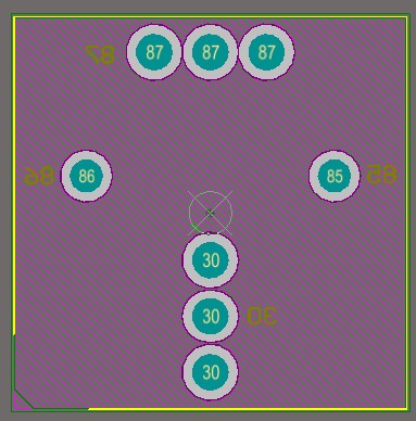
enter image description here

And the schematic symbol is as below:
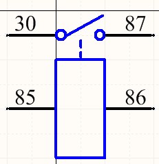
enter image description here

In my schematic, I don't give the two terminals any net, and they are floating (connect nothing). In the PCB editor, I want connect the three pads together using tracks, such as the three pads with the designator "87", but the Altium PCB editor prevent me doing this, the pads can't be connected!

I tried give a net to the terminal "87", then I can connect the three pads using tracks. I want to know what's the "strategy" behind this? I think if I give the pads same designator, they should be treated as just one pad, and should be "connectable". Right? Is there other easier method to make them connectable (I have 24 such relays, and it will be a hard work to give nets to the terminals)?

\$\endgroup\$
2
  • \$\begingroup\$ i have a same problem recently. I define three pin with different designator and connect each other in my schematic. Not a good solution but solve it. \$\endgroup\$
    – elektro
    Commented May 6, 2015 at 10:29
  • \$\begingroup\$ Why so many pins (87??)? Could you post the datasheet for the part please? \$\endgroup\$
    – DerStrom8
    Commented Sep 5, 2015 at 16:42

3 Answers 3

2
\$\begingroup\$

I once made a diode with a four-pin anode, all of which I wanted to connect together. You could connect all of the anode pins separately, but I would recommend giving them different pin names (i.e. 87a, 87b, 87c) and treating them as separate pins on the PCB layout. However, on the schematic, lay the three pins one on top of the other so it looks like just one pin. Altium will see a wire connected to the "one" visible pin as connected to all three pins, and will tell you to route all of their corresponding pads together. You will need to go into the pin editor on the schematic, though, and make sure you change the pin names and which pads they connect to. That's probably the most elegant solution.

\$\endgroup\$
2
  • \$\begingroup\$ This is the most 'elegant' way for now, though need some tricky. \$\endgroup\$
    – diverger
    Commented Oct 11, 2016 at 0:20
  • \$\begingroup\$ I realise this is now very old but in automotive relays, pin names like 87, 87a, 87b have specific meanings so the suggested scheme could cause confusion, so I'd suggest a variation of the scheme. \$\endgroup\$
    – John U
    Commented Dec 13, 2018 at 12:30
1
\$\begingroup\$

Three pads per contact implies that the relay is designed to carry large amounts of current. As such, you are going to want to use plenty of copper on the PCB to make the connection. Use either a trace that's wide enough to bridge all three pads when you connect it to the center pad, or a copper pour/polygon to surround all three pads with copper.

\$\endgroup\$
1
\$\begingroup\$

Two ideas:

1) Connect the pads together in footprint by having only a single pad that has 3 holes in it.

2) Have 3 pads all with the same designator. Connect a trace to one pad and then do a copper pour around them all attached to the net that you want them all connected to. The pour should then connect the pads together.

\$\endgroup\$

Your Answer

By clicking “Post Your Answer”, you agree to our terms of service and acknowledge you have read our privacy policy.

Not the answer you're looking for? Browse other questions tagged or ask your own question.