2
\$\begingroup\$

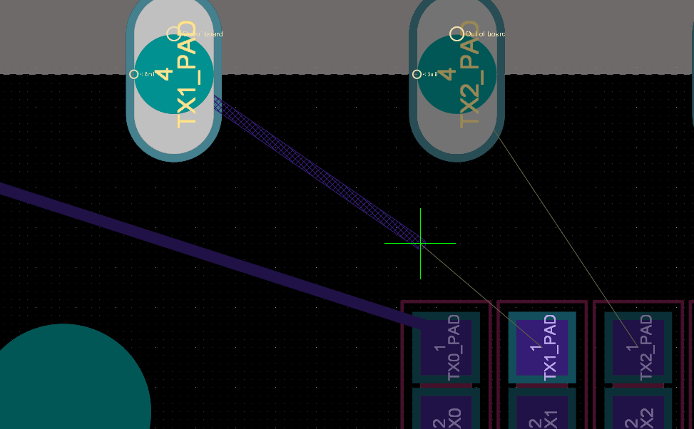
I use interactive routing with Altium to route components using Ctrl+W. This normally works well, but I have some castellated holes that are not in the schematic (I created them in the PCB file directly). They are set to the nets they are intended to, but I cannot interactively route to them. The tracks won't lock to the castellated pads:

enter image description here

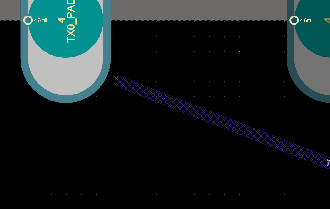
I have to do it the other way around, from them to the other components like so:

enter image description here

This is a concern because it starts the tracks from the center of the pad, where as I could lock them from their lower edge if I could connect with the interactive routing as seen in first image.

Is there a setting somewhere that could let me connect to pads like these that are not in the schematics?

\$\endgroup\$
2
  • \$\begingroup\$ If you end this trace without connecting it, and double click the trace for the net, what does it say? \$\endgroup\$ Commented Oct 14, 2021 at 1:52
  • 2
    \$\begingroup\$ If I recall correctly, you MUST route to the center of the pad, otherwise DRC will think the track is not connected to the pad. If you want a track to appear to come from the bottom of the pad, you need to place a short bit of track within the pad, then place a vertex as needed to have the track leave the pad at the desired place. \$\endgroup\$ Commented Oct 14, 2021 at 2:01

1 Answer 1

2
\$\begingroup\$

Here are some things you can try:

  1. Sometimes this behavior (not connecting to same-net objects) is inhibited by a clearance issue. Try momentarily setting Routing Options > Conflict Resolution to "Ignore Obstacles":

    Routing options > conflict resolution, ignore obstacles

    This will eliminate clearance rules as the reason it is not allowing the connection. (If this solves the issue, then you need to check your design rules to see if any are affecting the tracks/pads in question.)

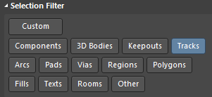
  2. There could be a track fragment hiding in the pad of a different net. Set the selection filter to track only:

    Selection filter, tracks only

    And select everything over and around the pads that are giving you the problem. If you see any pieces of track within the pad, delete them as they might be conflicting.

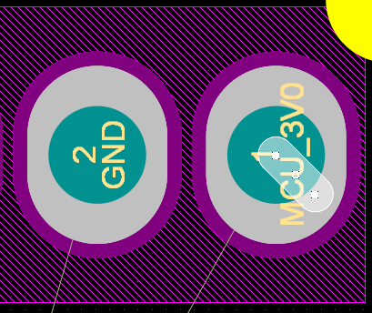
    For example, here's a pic showing a track fragment where the visible pieces exiting the pad were removed, but the remaining piece is still superimposed over the pad, and has a different net:

    Track fragment under pad

  3. If your castellated holes are on the PCB edge, it could be a Board Outline Clearance design rule preventing the track from routing to the pad. Even if the pad is not in the schematic, Altium should route to it if it is the same net. Try A) disabling any Board Outline Clearance rules if they exist, or B) move the castellated pad to another location (temporarily) to see if routing to it is allowed.

\$\endgroup\$
1
  • \$\begingroup\$ Option #3 where I moved the castellated pad to another location, routed it, then moved it back worked for me. That would be my preferred method since it didn't involve messing with rules. \$\endgroup\$
    – plu
    Commented Oct 4 at 19:32

Your Answer

By clicking “Post Your Answer”, you agree to our terms of service and acknowledge you have read our privacy policy.

Not the answer you're looking for? Browse other questions tagged or ask your own question.