0
\$\begingroup\$

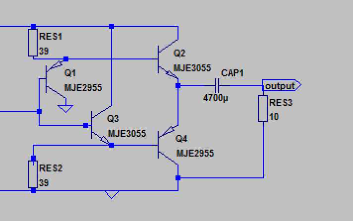
enter image description here In the circuit above a Class AB amplifier (this is one also called Class A+AB) can be seen with Q1 and Q3 used to get the current biasing voltage for Q2 and Q4. transistors Q2 and Q4 become hotter and hotter and requiring more and more current in the actual built circuit and in the end it reduces the output signal to 0. Are there easy changes that can be made to prevent this from happing? The power supply gives 10Volt.

EDIT: As some of you noticed, there's was no resistor shown at the output in the figure above, but it is added now.

\$\endgroup\$
13
  • \$\begingroup\$ The first obvious problem is that the collector of Q1 should be connected to the collector of Q4, exactly the same way that the collector of Q3 is connected to the collector of Q2. But the whole circuit looks wrong somehow - I'm going to need to look at it closer. \$\endgroup\$ Commented Mar 28, 2015 at 20:55
  • \$\begingroup\$ @DwayneReid The collector of Q3 and Q4 are both connected to ground. \$\endgroup\$
    – Coryak
    Commented Mar 28, 2015 at 21:01
  • \$\begingroup\$ It's overbiassed. I would have expected to see emitter resistors for Q2 and Q4 of around 0R1 to 0R33 each, and some NFB too. Strange circuit. There are plenty of good ones. I would start again. \$\endgroup\$
    – user207421
    Commented Mar 28, 2015 at 21:44
  • \$\begingroup\$ Small emitter resistors are the usual practise for output transistors \$\endgroup\$
    – Andy aka
    Commented Mar 28, 2015 at 22:30
  • 1
    \$\begingroup\$ The bias current through the non-existent emitter resistors. If you must persist, fit 0R33 between the emitter of Q2 and the output cap; same for Q4; and increase the values of the 39ohm resistors. You should measure 10-20mV across both emitter rspesistors in series. Orders of magnitude more than that is too much. In any event you need to add some NFB. And a Zobel network, 10R in series with 100nF from the junction of the emitter resistors to ground. I still agree with everybody else that there is something seriously wrong with this circuit. For the 3rd or 4th time, where did you get it? \$\endgroup\$
    – user207421
    Commented Mar 29, 2015 at 0:02

1 Answer 1

1
\$\begingroup\$

It appears that you are using the B-E junctions of Q1 and Q3 to provide the bias for Q2 and Q4, respectively. This will only work if the four transistors are coupled thermally so that they are all at the same temperature.

Also, the value of 39 for RES1 and RES2 is ridiculously low. What are the operating voltages of this amplifier?

Overall, this is a very poor circuit. Where did you get it?

\$\endgroup\$
4
  • \$\begingroup\$ Does that mean glueing those transistors together? Will that work with those power transistors? The input and output voltage is around 5V DC with an amplitude of around 3V. So the signal goes from 2V until 8V \$\endgroup\$
    – Coryak
    Commented Mar 28, 2015 at 21:22
  • 1
    \$\begingroup\$ No, don't glue them together. First, get a better circuit to work with. \$\endgroup\$
    – Dave Tweed
    Commented Mar 28, 2015 at 22:52
  • \$\begingroup\$ So you think there is not an easy way to fix this circuit? \$\endgroup\$
    – Coryak
    Commented Mar 28, 2015 at 23:26
  • \$\begingroup\$ Power supply gives 10V. \$\endgroup\$
    – Coryak
    Commented Mar 28, 2015 at 23:53

Your Answer

By clicking “Post Your Answer”, you agree to our terms of service and acknowledge you have read our privacy policy.

Not the answer you're looking for? Browse other questions tagged or ask your own question.