22
\$\begingroup\$

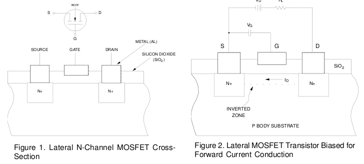
Looking carefully at this diagram of one type of MOSFET:

enter image description here

(found in this application note)

We can see the device is virtually symmetrical. What makes the gate reference itself to the source and not the drain?

Also, why would the gate oxide break down at 20V Vgs and not 20V Vgd?

(Not a homework question. Just curiosity.)

\$\endgroup\$
3
  • 1
    \$\begingroup\$ I know that most JFETs are indeed pretty much symmetrical in the way you describe, and it doesn't really matter which end is used as the source and which is the drain. I'm not positive if the same thing applies to lateral MOSFETS, though. Vertical MOSFETs contain a parasitic body diode and won't work properly when connected "backwards." \$\endgroup\$
    – MattyZ
    Commented Jul 2, 2011 at 23:23
  • 1
    \$\begingroup\$ @Bitrex True, a power MOS won't work backwards normally. But if you can short out the diode if the drain-source channel has a low enough resistance and then the channel is conducting current, not the diode. This is used in active bridge rectifiers and in other devices which require controlled rectification. But you are limited to about 0.5V backwards before things go wrong ;). \$\endgroup\$
    – Thomas O
    Commented Jul 3, 2011 at 0:13
  • \$\begingroup\$ If you are using a MOSFET as part of a synchronous rectifier, you can put a Schottky diode in parallel with the MOSFET's body diode to protect the MOSFET. The body diode is usually pretty weak. \$\endgroup\$ Commented Jul 4, 2011 at 13:03

5 Answers 5

9
\$\begingroup\$

Because the Figure 1 you posted refers to a 4-terminal device, not a 3-terminal one. If you look at the schematic symbol in Figure 1, you'll note that the body terminal is a separate terminal not connected to the source terminal. MOSFETs for sale are almost always 3-terminal devices where source and body are connected together.

If memory serves me right (not 100% sure -- seems to be corroborated by this handout), in a 4-terminal device there is no difference between source and drain, and it is the gate-body voltage that determines the on-state of the channel -- with the caveat that the body is supposed to be the most negative voltage in the circuit for an N-channel device, or most positive voltage in the circuit for a P-channel device.

(edit: found a reference for MOSFET device physics. The source-drain behavior is still symmetric, but depends on both gate-source and gate-drain voltages. In N-channel, if both are negative, the channel is nonconducting. If one is greater than the threshold voltage, then you get saturation behavior (constant-current). If both are greater than the threshold voltage, you get triode behavior (constant-resistance). The body/bulk/substrate still needs to be the most negative voltage in the circuit, so to get the reversed behavior in a circuit, body + drain would need to be tied together.

In a P-channel device, this polarity is reversed.)

Look carefully at the conventional schematic symbols for N- and P-channel MOSFETs (from Wikipedia):

n-channel p-channel

and the Wikipedia figure on MOSFET functioning, and you'll see the body-source connection.

\$\endgroup\$
7
  • \$\begingroup\$ Even in 4 terminal the gate source voltage determines state of the channel. So what you have wrote about gate-body is not true. The source - body voltage will modulate threshold voltage of the device. For example for NMOS if Vs is above Vb then one will need bigger Vgs to turn on device (the body effect). \$\endgroup\$ Commented Jul 4, 2011 at 11:46
  • \$\begingroup\$ @mazurnification: where's your reference for this? and why is it gate-source rather than gate-drain or gate-body? I tried to find reference material either way and could not. \$\endgroup\$
    – Jason S
    Commented Jul 4, 2011 at 12:16
  • 1
    \$\begingroup\$ Just found this reference: doe.carleton.ca/~tjs/21-mosfetop.pdf which states channel fields based on Vgb, not Vgs (until Vsb = 0 at which point Vgs = Vgb). So I'm not going to change my answer until I see evidence that there's something special about the source terminal. I wouldn't be surprised if the body effect of modulating threshold voltage is only true if the source-body connection is a low-impedance fixed voltage, and that it is equivalent to the equations governing Vgb. \$\endgroup\$
    – Jason S
    Commented Jul 4, 2011 at 12:37
  • \$\begingroup\$ OK, found something that refers to gate-source and gate-drain voltages. \$\endgroup\$
    – Jason S
    Commented Jul 4, 2011 at 12:43
  • \$\begingroup\$ The key is Vgb. The whole point of a MOSFET is for the electric field created between the gate and substrate to imbalance the distribution of charge carriers, changing the impedance of the channel between source and drain. However, since source and substrate are generally connected together (see schematic symbol), Vgs is the same as Vgb. If you don't want the channel to be the same as the substrate, you have to create a well structure, which looks like a reverse-biased diode from channel to substrate. Remember that you can create structures in ICs that are unfeasible in discrete parts. \$\endgroup\$ Commented Jul 4, 2011 at 13:01
9
\$\begingroup\$

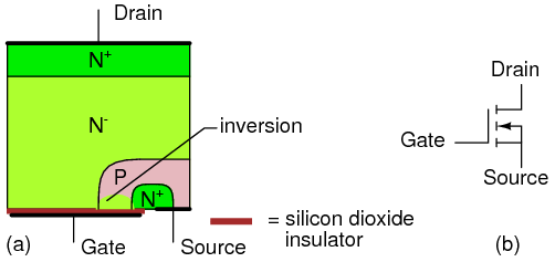
The symmetrical cross-section as it's usually drawn doesn't quite agree with the actual structure, which is highly asymmetrical. Actually it looks more like this:

enter image description here

with a much larger area for the drain than for the source. It's possible to specify \$I_D\$ vs \$V_{GD}\$, but you'll get a totally different relationship, which is rather irrelevant in common source applications, which are the most used.

\$\endgroup\$
8
  • \$\begingroup\$ Are you sure this is not just a vertical MOS? Is a lateral MOS different? \$\endgroup\$
    – Thomas O
    Commented Jul 4, 2011 at 7:15
  • \$\begingroup\$ @Thomas - a V-MOSFET looks different: allaboutcircuits.com/vol_3/chpt_2/10.html. Anyway, they are very much asymmetical, so even if the picture looks different, the explanation still stands. \$\endgroup\$
    – stevenvh
    Commented Jul 4, 2011 at 7:47
  • \$\begingroup\$ This structure is frequently used for discrete MOSFETs. The symmetric structure is usually used for MOSFETs on integrated circuits, since they can't all share a drain. \$\endgroup\$ Commented Jul 4, 2011 at 12:55
  • \$\begingroup\$ yep mosfet from integrated circuit most likely will be fully symmetrical \$\endgroup\$ Commented Jul 4, 2011 at 14:04
  • \$\begingroup\$ @MikeDeSimone, @mazurnification - It will look different for ICs, but I'm still not quite sure those will be symmetrical. \$\endgroup\$
    – stevenvh
    Commented Jul 4, 2011 at 15:13
3
\$\begingroup\$

The operation of given MOSFET is determined by voltages on their respective electrodes (Drain, Source, Gate, Body).

By textbook convention in NMOS out of two electrodes "connected to the channel" (between which in "normal" circumstances current flows) the one connected to the lower potential is called source and the one connected to higher is drain. The opposite is true for PMOS (higher potential source, lower potential drain).

Then using this convention all equations or texts describing device operation is presented. This implies that whenever author of the text about NMOS says something about transistor source (s)he thinks about electrode connected to lower potential.

Now the device manufacturers most probably will choose to call source/drain pins in their devices based on intended configuration in which MOSFET will be \placed in final circuitry. For example in NMOS pin usually connected to lower potential will be called source.

So this leaves two cases:

A) MOS device is symmetrical - this is a case for vast majority of technologies in which VLSI IC are manufactured.

B) MOS device is asymetrical (vmos example) - this is a case for some (most?) discrete power devices

In case of A) - it does not matter which side of the transistor is connected to highier/lower potential. Device will perform exactly the same in both cases (and which electrode to call source and which drain is just convention).

In case of B) - it does matter (obviously) which side of device is connected to which potential since the device is optimized to work in given configuration. This will mean that "equations" describing device operation will be different in case the pin called "source" is connected to lower voltage then compared to the case where it is connected to higher.

In your example device was most likely engineered to be asymmetrical in order to optimize certain parameters. The "gate-source" brake-down voltage was lowered as a trade-off in order to get better control on channel current when control voltage is applied between pins called gate and source.

Edit: Since there is quite some comments regarding symmetry of the mos, here goes quote from Behzad Razavi "Design of the analog CMOS integrated citcuits" p.12

quote

\$\endgroup\$
5
  • \$\begingroup\$ I'm not sure how simulation technologies have changed over the years, but by my understanding, as of ten years or so ago, many simulators essentially wanted the source and drain nodes labeled to identify which node should be viewed as affecting the other. Essentially, the label "source" meant "cause", and "drain" meant "effect", and the circuit should be laid out such that if the drain/effect of an NFET has a path to ground, the source/cause should either have a path to VSS or be a "don't-care" (likewise for PFETs and VDD). If a circuit can be laid out to meet that criterion, then... \$\endgroup\$
    – supercat
    Commented Jul 6, 2011 at 15:38
  • \$\begingroup\$ ...the simulator can for each clock phase arrange all the nodes in a sequence such that every node only needs to be evaluated once, and no node will be affected by a "downstream" node (until the next clock phase, which will have the nodes in a different arrangement). Certain circuits using pass-gates would require reversing source and drain labels to help the simulator, but in general the causality restrictions would make it practical to simulate circuits faster than would otherwise be possible. \$\endgroup\$
    – supercat
    Commented Jul 6, 2011 at 15:42
  • \$\begingroup\$ @supercat - there are few "levels" of simulators. Starting from physical (tcad for example) where one is actual simulating electrical and magnetic fields, then electrical (all SPICE like) to the functional (verilog, vhdl, verilogA etc). All of them were already very advanced 10 years ago. The one you mention look kind of like functional "event driven simulator" (like verilog one) but I have not seen such technique applied to the actual transistors (well maybe in so called "fast spice"). The point is that electrical (spice) can handle symmetry of the mosfet easily ... \$\endgroup\$ Commented Jul 6, 2011 at 19:22
  • \$\begingroup\$ Certainly it's possible to simulate circuits where causes and effects don't form a directed acyclic graph, and the increases in computing horsepower during the last ten years have made full simulation practical for larger designs than would have been possible ten years ago. I wouldn't be surprised, however, if circuits which can be cause-effect mapped, however, would be amenable to faster simulation than those which cannot, or if informing a simulator that a certain transistor should only be called upon to pass current in one direction might help catch mistakes... \$\endgroup\$
    – supercat
    Commented Jul 6, 2011 at 19:31
  • \$\begingroup\$ ...where it ends up passing current the other way. Of course, with static logic such problems would usually cause a VDD-VSS short, but in dynamic logic it could cause problems without a VDD-VSS short. Not sure how much dynamic logic is still used outside DRAMs, though (is it?) My main point was that labeling source and drain as a habit would have benefited at least some simulators. \$\endgroup\$
    – supercat
    Commented Jul 6, 2011 at 19:34
0
\$\begingroup\$

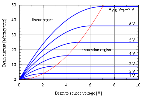
A MOSFET requires two things for current to flow: charge carriers in the channel, and a voltage gradient between the source and drain. So, we have a three dimensional behavior space to look at. The drain-source characteristic looks something like this: enter image description here

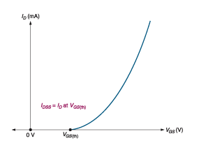
Let's assume we have an nmos transistor, and the bulk and source are at 0V. Let's also set the drain voltage high, say 5V. If we sweep the gate voltage, we'd get something that looks like this:

bulk

In order for there to be substantial amounts of charge carriers in the channel, we need a depletion region connecting the source and drain, and we also need to pull a bunch of carriers out of the source. If the source and gate are the same voltage, this means most of the channel is also essentially the same voltage as the source, and the carriers need to diffuse most of the way across the transistor before they can "fall" into the drain. If the gate-source voltage is high enough, the voltage gradient will be more significant near the source, and the carriers will be pulled into the channel, allowing a higher population.

\$\endgroup\$
1
  • \$\begingroup\$ This explains the MOSFET theory of operation, but doesn't say anything about possible symmetry, and doesn't answer Thomas' question if source and drain are interchangeable. \$\endgroup\$
    – stevenvh
    Commented Jul 6, 2011 at 14:01
0
\$\begingroup\$

My 2 cents worth: Comparing to bipolars, I know you may swap C and E and it's still working, but with lower hFE and different voltage ratings: VBE allowed to be max around 5 to 7V usually; VCB same as VCE or more (cf. e.g. BC556 datasheet from Fairchild, which specifies VCBO, which is even higher than VCEO). Physically there's a (big) difference between C and E (size, shape and/or doping) which explains the asymmetry in the figures. And I've seen this in the lab as well. It happens now and again that someone swaps C and E by accident and are surprised it still works but not very well.

Would be interesting if someone was to get a graph of ID (and RDSon) vs VGD for a (power N-channel MOSFET. Haven't got lab access presently.

\$\endgroup\$

Your Answer

By clicking “Post Your Answer”, you agree to our terms of service and acknowledge you have read our privacy policy.

Not the answer you're looking for? Browse other questions tagged or ask your own question.