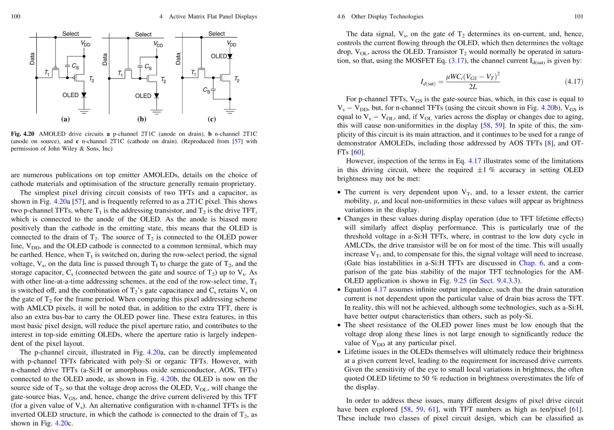
My question was incorrectly posed, because I didn't include the capacitor connecting the gate to one of the terminal. So in fact this question is regarding common source vs common drain comparison...

-
\$\begingroup\$ There is a lot of confusion here, are you talking about the bulk of the transistor as the 4th terminal? \$\endgroup\$– JuanCommented Jul 18, 2019 at 2:06
2 Answers
For a planar MOSFET like this the designation of the source and drain is not determined by the physical layout of the transistor...the layout is symmetric. If it is an NMOS then at any given instant the terminal with the lower voltage is the source and the terminal with the higher voltage is the drain. So, \$V_{GS}\$ has a consistent meaning regardless of which physical "end" of the transistor you connect to.
-
\$\begingroup\$ I understand that, and yet it still matters which terminal in the circuit topology, that the load is added to. You didn't understand my question I believe. I added the text book describing the exact issue.... \$\endgroup\$– CamCommented Jul 18, 2019 at 3:22
-
\$\begingroup\$ I'm sorry but your question remains unclear to me. You ask about connecting to source vs drain, and then you start asking about a fourth terminal. You write a long, somewhat disjointed, section of text and then ask a very vague question such as "why does this matter?" without being specific about what this is. \$\endgroup\$ Commented Jul 18, 2019 at 11:19
-
\$\begingroup\$ Sorry Elliot, please give me another shot. For a given current direction and given transistor channel doping, I don't understand why when a load is connected to the drain side or the source side it makes a difference to the overall current. Isn't the average electric field across the channel the same? This is the same thing as asking: for a given current direction and for given placement of the same load (drain or source side) then what difference does it make if the majority carrier is electron or hole in the channel? This is what the textbook is saying comparing circuit (a) to circuit (b) \$\endgroup\$– CamCommented Jul 18, 2019 at 19:38
you are confusing a lot of concepts, in my opinion. You should forget about thin film and OLED for a split second and think about how a transistor and how a diode is supposed to work, what the difference between a pnp and npn junction layout and why the current has to go in a certain direction.
You are referring to the bulk terminal of the transistor by any chance? not having a terminal to it does not mean it stops existing.
If you look at most diagrams of how a MOSFET is laid out it is essentially symmetrical, in discrete components source is shorted to the bulk, I cannot say for certain this is what is happening in your case, The real thing that controls the turn on is gate to bulk voltage, source if often shorted to that so a lot of literature says that gate to source voltage is responsible for the turn on.
The current direction of the N and P transistors is mostly due to the fact that the bulk itself is made of a different material.
your Vgd questions has been answered before so I will lead you to that for a more detailed answer here
the answer is not as detailed as it could be, but you can go on forever on this topic.
-
\$\begingroup\$ It's not an issue of terminal. A thin film transistor is on an insulating substrate. You need to read more carefully, I have read the answer you linked to, it refers again to a 4th terminal. Are you saying the glass substrate has a different fermi level from the channel, and this energy difference is different for p and n channel? Then say so clearly...I may not be as confused as you are :P \$\endgroup\$– CamCommented Jul 18, 2019 at 3:24
-
\$\begingroup\$ See the text book page I added to understand the issue. \$\endgroup\$– CamCommented Jul 18, 2019 at 3:26
-
\$\begingroup\$ You only care about the reasoning behind the location of the OLED? the reason as far as I know is to compensate for the threshold voltage of the first transistor(T1(Vt)) by adding the second transistor voltage (T2(Vt)) to the data voltage stored in the capacitor. besides that you are correct, there is no difference in where you place the OLED. source for what I am saying (ikee.lib.auth.gr/record/292357/files/GRI-2017-19696.pdf) page 53 this is assuming T1 and T2 are identical TFTs \$\endgroup\$– JuanCommented Jul 18, 2019 at 4:00
-
\$\begingroup\$ Hi Juan, but there is a difference, this is what the textbook pages are explaining in my post. If you keep the circuit the same (same OLED position, same current direction), and change from p type to n type transistor (assuming transistor spec are identical), then the overall current becomes sensitive to the OLED resistance in one type, but not sensitive to OLED resistance with the other ttype. We can ignore the OLED properties and assume a simple linear resistor. \$\endgroup\$– CamCommented Jul 18, 2019 at 19:42
