5
\$\begingroup\$

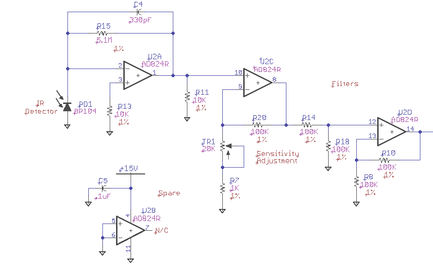
I have the front end of a photodiode detector. What is the point of the third op amp? The output from U2C gets divided in half from R14 and R18, then it just gets double by U2D again.

Is there a reason for this other than just using the rest of the 4 stage op amp circuitry? Are the two acting as a stabilizer for the signal?

When would you want to use cascading (I believe this is the correct terminology) op amps?

enter image description here

Background info: I'm looking to possibly replicate it with another detector but am asking questions about the circuit since it was designed way before my time. I'm wondering if my detector should use one op amp or use cascading op amps.

\$\endgroup\$
4
  • \$\begingroup\$ Before I start thinking about an answer once I'm done cooking and eating dinner: If you build this, better to bias U2B such that its output swings hard to a signal. With such small signals on the same chip as to needing 5MOhm, you don't want any unstable components risking cross talked noise. \$\endgroup\$
    – Asmyldof
    Commented Jun 30, 2015 at 19:38
  • \$\begingroup\$ Which one is "Third"? \$\endgroup\$
    – Eugene Sh.
    Commented Jun 30, 2015 at 19:39
  • \$\begingroup\$ Eugene (and slightly Asmyldof)- U2A is the first, U2C is the second, U2D is the third. U2B isn't used. \$\endgroup\$
    – Luke
    Commented Jun 30, 2015 at 19:43
  • \$\begingroup\$ Regarding the use of the circuit, it's currently in use at my company. I'm looking to possibly replicate it with as another detector but am asking questions about the circuit since it was designed way before my time. \$\endgroup\$
    – Luke
    Commented Jun 30, 2015 at 19:46

3 Answers 3

4
\$\begingroup\$

I don't see much reason to have it. Perhaps it was once used for "filters" as the annotation suggests.

Nor do I see a reason for R13.

This circuit could probably be reduced to a single op-amp (with some improvement to the stability).

\$\endgroup\$
1
  • 1
    \$\begingroup\$ This is what I was thinking but wasn't 100% sure if there was some deeper reason that I didn't know about. \$\endgroup\$
    – Luke
    Commented Jun 30, 2015 at 20:00
2
\$\begingroup\$

The only possible reason for the series of op-amps in this set-up could be "filters" in the unity-gain region of the op-amps, but that would not be a very smart way to filter.

It's also possible the U2D has a capacitor somewhere, because the composite maths of filtering in the post-amplifier became too complex for the designer around U2C and it is simply forgotten in the drawing that you have.

As Spehro says it's also possible this capacitor was removed and the schematic updated to the new situation, for servicing reasons.

Any of that is possible, and can only truly be answered with a crystal ball or an original designer.

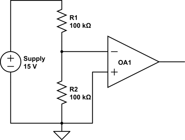
To quickly rehash my comment: When you use a chip with multiple Op-Amps and you have one of them working with nA-scale currents, so as to need a 5M feedback resistor, you should prefer connecting the op-amp inputs such that the output strongly biasses to one of the rails, to prevent on-chip noise created by the unused op-amp(s). Such as, for example:
schematic

simulate this circuit – Schematic created using CircuitLab

Would always force the op-amp towards the ground rail (often the easiest one for an op-amp) while the circuit is powered.

Whether you will need any active filtering other than the feedback-filtering by the capacitor C4 can only be said with knowledge of the signals coming in, what should go out and what components you're using.

The second op-amp (U2C) may be a valid addition, though possibly with a fixed amplification of 10 to 100 (potentiometers are noisy as well! though to a very limited degree at 20x amplificatoin), to reduce the noise sensitivity of sensor leads or to increase the responsiveness of the total circuit, again depending on the parameters you are designing with.

The best thing to do is to just start working sensibly from what your sensor does towards what you need at your output and leaving what is currently in place out of it, if it uses a different sensor and different tactics from a different time. You can look at some points of the existing system if you can find behaviours that explain this schematic, such as noise or biasing, but if you find none (which I suspect): Start over and be sure to test what you calculate before making it a final part of your legacy.
\$\endgroup\$
2
  • \$\begingroup\$ I'm getting around to reading this after my long weekend. But regarding the Cap after U2D, there is a .68uF after the opamp output. I didn't think it needed to be included. \$\endgroup\$
    – Luke
    Commented Jul 6, 2015 at 15:42
  • \$\begingroup\$ Thank you very much for the detailed answer. I appreciate the time you spent (I hope I didn't cut your dinner short!). The circuit I'm using won't use a POT. I was going to experiment with using a second op amp but similar to U2C going to U2D. Where the circuit cuts the output in half, then doubles it again. \$\endgroup\$
    – Luke
    Commented Jul 6, 2015 at 15:54
1
\$\begingroup\$

Since U2D is part of a differential amplifier of gain 1, with one input grounded, perhaps its purpose was initially to compensate for any offset in the signal, caused either by dark/leakage current in the photodiode, or input offset voltages of the two preceding stages.

That would only make sense if the grounded input (bottom of R8) were at some potential other than 0V (by employing another potentiometer, perhaps), but it's the only reason I can think of why this last stage exists at all.

\$\endgroup\$

Your Answer

By clicking “Post Your Answer”, you agree to our terms of service and acknowledge you have read our privacy policy.

Not the answer you're looking for? Browse other questions tagged or ask your own question.