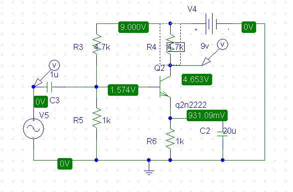
Your choices of components look good.
Ideally Vc_DC shouild Vbattery/2 and the 4.635V you see is entirely close enough to Vbattery/2 = 9V/2 = 4.5V/2 for this purpose.
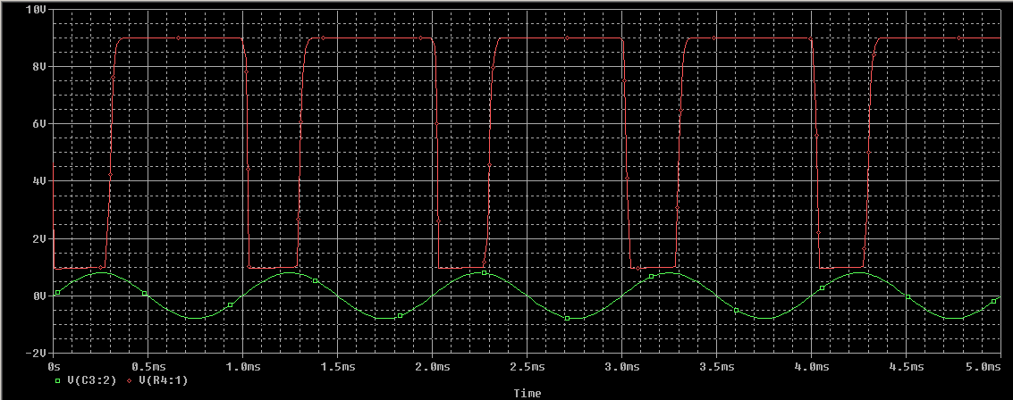
(1) As shown the gain is very high.
It is ABOUT Rc/Reinternal
where Reinternial is the effective emitter resistamce of the transistor and is approximately equal to 26/Ie_ma.
The reason for this formula is based on the behaviour of a silicon junction with current - just accept it for now.
Here Ic ~= Ie~= V_r6/R6 = 0.93 mA.
So Reinternal = 26/0.3 = 28 Ohms.
Gain ~= Rc/Reinternal = 4.7k/28 =~ 168
For 4.5V max swing on collector Vin_half_cycle_peak = 4.5/168 = 27 mV
So an input of about 20 mV AC 1/2 cycle peak will about give maximum allowable Vc.
As your simulator gives 5V peak for a 5V signal try Vin = 20 mV.
(2) Next, remove C2.
The gain, as you probably know is ~= R4/R6 = 4.7k/1k = 4.7 ~= 5
so with ~- 4.5V max swing at the collector you can expect the transistor to be driven into on or off modes by some of the saignal. c
With a gain of 5 and swing of 4.5V the max Von you can tolerate is ABOUT 4.5/5 = 0.9V.
If you drive it with say 0.8V 1/2 peak or less the output will "make sense"
At present when Vin is too high the transistor turns hard on.


