6
\$\begingroup\$

I am trying to create a UART receiver in Verilog for my FPGA. I was following this guide http://www.fpga4fun.com/SerialInterface4.html

According to it the standard practice for asynchronous communication is to oversample the signal at 16 times the BAUD rate. This makes sense to me since I would need to do this to detect the first drop quickly and synchronize with the transmitting clock.

What I am wondering is why not just sample at the same frequency as the clock on my FPGA which is a lot fast than 16x the BAUD (my clock is 100 MHz). Is there any harm in doing this? I know it would probably just consume more power, but would it work or is there something I am missing?

\$\endgroup\$

5 Answers 5

5
\$\begingroup\$

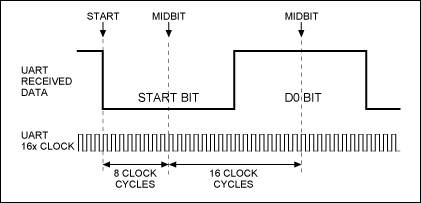
I've sampled at 8 times on one job and it was OK so there is no rule dictating that 16 is the magic number so sampling higher than this is not a problem in anthing other than handling bigger numbers in hardware. Here's a the 16x counter idea: -

enter image description here

From the falling edge of the start bit you "find" the start-bit's "middle" by counting to 8 then, each count of 16 thereafter you "sample" the UART received data to recreate the byte (or bytes) transmitted. Clearly if you had a 32x counter you'd get a tad more accuracy in determining the centre-point of the bit and counting at a higher rate is going to work but the numbers get bigger and the power consumption rise.

\$\endgroup\$
3
  • \$\begingroup\$ I just figured it is easier to just sample at the 100 Mhz clock I already have rather than create a module to divide it up. \$\endgroup\$
    – chasep255
    Commented Dec 25, 2015 at 14:52
  • \$\begingroup\$ I understand but you have to weigh up hardware stuff like - is it more efficient to divide down to a lower frequency and use smaller counts with less hardware and less current consumption. \$\endgroup\$
    – Andy aka
    Commented Dec 25, 2015 at 14:54
  • 3
    \$\begingroup\$ Let's say your UART is working at 9600 baud. Then one data cell is 104 usec. A 100 MHz clock will require 104,000 clock cycles to deal with the UART data, and this in turn needs a 17-bit counter. You may find this a bit wasteful of resources, and performing the necessary logic at 100 MHz may be a pain, but it's your choice. This sort of tradeoff (extra FPGA resources vs external slow clock) is exactly what design engineers do for a living. And, of course, there's nothing preventing you from dividing down your 100 MHz internally to make the UART logic more compact. \$\endgroup\$ Commented Dec 25, 2015 at 15:58
4
\$\begingroup\$

For a very simple UART receiver, it really doesn't matter all that much which way you go.

However, many UART designs need to be both robust and flexible, and that drives the design toward creating a 16x clock (or clock enable) signal.

For robustness, it is advantageous to sample each bit multiple times near the center of the bit and then take a vote among the multiple samples in order to minimize the effects of noise. For example, it's common to take samples at 7/16, 8/16 and 9/16 through the bit and take whichever value appears most often. If you tried to take three adjacent samples at 100 MHz, they're almost guaranteed to have the same value even if they are a glitch, so you want them spaced farther apart.

For flexibility — for example, needing to support many different possible baud rates — you want to have just one parameter that controls the baud rate. If you have several different internal delays that depend on the baud rate (i.e., 1 bit period, 1/2 bit period, 7/16 bit period, etc.), the logic becomes more complex than if you have one state machine that runs at, say, 1/16 the bit period. In that case, all of the different delays scale with the one parameter automatically.

\$\endgroup\$
4
\$\begingroup\$

Because UART is asynchronous it can only be sampled by over-sampling.

There is a lower boundary for over-sampling defined by the the possible error made by missing the falling edge of the start bit. So by a 8x over-sampling a possible mismatch of the falling edge causes an max. error of 12.5 %. 16x over sampling reduces the error to 6 %.

The upper boundary is limited by your investment in hardware ressources. No one wants to use a 32 bit counter :).

\$\endgroup\$
1
\$\begingroup\$

If you analyze the Verilog code of the link you provided, there is an assertion segment:

generate if(ClkFrequency<Baud*8 && (ClkFrequency % Baud!=0)) ASSERTION_ERROR PARAMETER_OUT_OF_RANGE("Frequency incompatible with requested Baud rate"); endgenerate

Again if you look at the code there are two constant parameters for clock frequency and baud rate:

parameter ClkFrequency = 25000000; // 25MHz parameter Baud = 115200;

Well first of all the code will throw assertion with these constants! Because 25_000_000 can not be divided by 115200 with no residue. So you need some wierd clock frequencies to implement such UART logic with your FPGA.

I want to ask a question for x8 or x16 supporters, can you communicate with a device using UART with 1_843_200 bps baud rate with even a high clock frequency such as 100 MHz? Well with x16 sampling, you need 1/(BAUDx16) second tick, which is 33.908 ns. But with 100 MHz clock freq your resolution is 10 ns, so with counting up to 3, you get 30 ns. So you will generate a baud tick of 30 ns instead of 33.908 ns, where the error rate is 33.908/30 = 13% !!!

Okay you can say well for this case I can use x8 oversampling. So I need to generate 1/(BAUDx8) second tick, which is 67.81 ns. This time the error rate is 67.817/70 = 3%. Then I will ask what if you have 50 MHz instead of 100 MHz?

IMHO, because UART is an old protocol, at that time using less resources for circuit was crucial. However, today with thousands of gates in an FPGA, most of the times adaptation to newer requirements quickly and modularity gains importance, especially for small low-end protocols such as UART, SPI, I2C etc. Therefore, sampling each time of RX signal gives you the ability to communicate higher baud rates with little extra resources, which you have huge amount of inside FPGAs nowadays.

By the way, believe it or not but x8 or x16 tick generation circuit also spent resources of FPGAs! It is not a free tick signal.

So my answer for the question "Is there any harm in doing this?", is NO, even you will have more flexibility and achieve higher baud rates.

Regards,

\$\endgroup\$
1
\$\begingroup\$

Is this for demo purposes, a production design, or a reusable IP block? If for demo purposes, just do whatever you can get working. If for production, if you have plenty of FPGA resources, just use the 100MHz and huge counters and lots of logic. For reusable IP (or limited resource production design), you will want to assume the use of an FPGA PLL/DLL/ClockMgr to produce a much slower clock for the UART logic and reduce the FPGA resource utilization. The critical functional concern is that your receiving logic can tolerate the drift between transmitting and receiving clock domains (worst case delta between clock source freq+ppms) over the full duration of every possible message length and still accurately sample every bit.

\$\endgroup\$

Your Answer

By clicking “Post Your Answer”, you agree to our terms of service and acknowledge you have read our privacy policy.

Not the answer you're looking for? Browse other questions tagged or ask your own question.