4
\$\begingroup\$

New Intel and AMD processor feature processors with 14-22nm gate lengths, and this information is widely available. However, when it comes to microprocessors (PIC, ATMEGA) I have not been able to find this information. Is it "classified" ?

As to ARM processors, since ARM is an architecture, who defines the technology to be used when manufacturing say an Cortex-A8? I used this example because the Beaglebone Black uses a ARM Cortex-M8 manufactured by Texas Instruments, so which of these entities sets the technology? Again, unable to find information related to this.

\$\endgroup\$
3
  • \$\begingroup\$ TI has an ARM license, they are the ones who choose what process to build it on. IIRC, they don't have an architecture license though. This applies to your BeagleBone question \$\endgroup\$ Commented Jan 3, 2016 at 19:03
  • \$\begingroup\$ The most readily available data for Cortex-A processes is probably the nVidia Tegra, for the same reason as with Intel and AMD CPUs. \$\endgroup\$
    – jaskij
    Commented Jan 3, 2016 at 20:46
  • 1
    \$\begingroup\$ Just to precise, PIC/Atmega/MSP ecc are microcontrollers, AMD/Intel microprocessors \$\endgroup\$
    – thexeno
    Commented Jan 3, 2016 at 22:00

4 Answers 4

6
\$\begingroup\$

New Intel and AMD processor feature processors with 14-22nm gate lengths, and this information is widely available.

The reason this is so highly publicized is probably historic more than anything, relating to Moore's law. There probably isn't a company more ingrained in the computer market than Intel (Gordon Moore's company). They have been pushing the process envelope for years. Regardless of how we got here, it's become a race to the bottom between the foundries to see who can get to the smallest process node first. Whoever that is, is going to have a big payday, making the bleeding edge SOCs of that time.

However, when it comes to microprocessors (PIC, ATMEGA) I have not been able to find this information. Is it "classified" ?

It's not that it's classified, it's more than no one cares. Wind the block back a few years and the choice between AMD and Intel for your computer when you bought it was a big deal. No one cares whether there is a PIC or ATmega in their toaster oven, let alone what process node it was made in. The designers don't care either. My company uses PIC almost exclusively. Process node was not a variable when that decision was made. It was all based on cost, tools, availability, and support. For that reason, Atmel and Microchip are probably still making those lines of products in a micron scale fab because it's paid for.

As to ARM processors, since ARM is an architecture, who defines the technology to be used when manufacturing say an Cortex-A8?

ARM only licenses their core, they have no say in what process node is used.

I used this example because the Beaglebone Black uses a ARM Cortex-M8 manufactured by Texas Instruments, so which of these entities sets the technology? Again, unable to find information related to this.

Again, you're not going to find that information because the people buying those chips don't care. TI may tell you if you ask them directly (maybe only after you buy a few thousand chips), but they have nothing to gain from publishing it.

\$\endgroup\$
5
  • \$\begingroup\$ Clear explanation. I intended to use the example of smaller gate lengths as a way to demonstrate how new manufacturing techniques (hence smaller uC and sensors) were an enabling factor for the IoT. Now, I'm not so sure I can draw a parallelism. \$\endgroup\$
    – AmiguelS
    Commented Jan 3, 2016 at 19:40
  • \$\begingroup\$ @AmiguelS IoT was enabled by a perfect storm. It's less technically interesting, but what about taking a look at the proliferation of low cost wireless internet? There should be tons of consumer data on that. \$\endgroup\$
    – Matt Young
    Commented Jan 3, 2016 at 20:03
  • \$\begingroup\$ Yes there is, tons and tons of it. Already have that covered. I'm considering and identifying the various of the factors that created that perfect storm, as you mention. \$\endgroup\$
    – AmiguelS
    Commented Jan 3, 2016 at 20:06
  • 1
    \$\begingroup\$ @AmiguelS: 10 years ago people thought that the proliferation of home PCs would usher the IoT universe (back then it wasn't called IoT, it was called the Digital Hub - which has since evolved to mean mostly media players, 10 years before that it was called Home Automation which have since evolved to mean timed light dimmers and home alarms). Today we see that the proliferation of smartphones have led to the commercialisation of much more TCP/UDP controlled gadgets (but it's mostly toys). \$\endgroup\$
    – slebetman
    Commented Jan 4, 2016 at 2:52
  • \$\begingroup\$ @AmiguelS If you haven't moved on from this paper by now, I thought of another angle to take. As the nanotechnology process nodes moved into production, the old micron scale fabs, that were already paid for, were obsolete. Running 8-bit microcontrollers and sensors that could be fabricated at those nodes was cheap compared to the new nanoscale nodes. Nanoscale fabs cost billions to build. That data is fairly available. Having the fabs already paid for, and with a large part of their capacity now free, the costs of microcontrollers fell. \$\endgroup\$
    – Matt Young
    Commented Jan 9, 2016 at 2:47
4
\$\begingroup\$

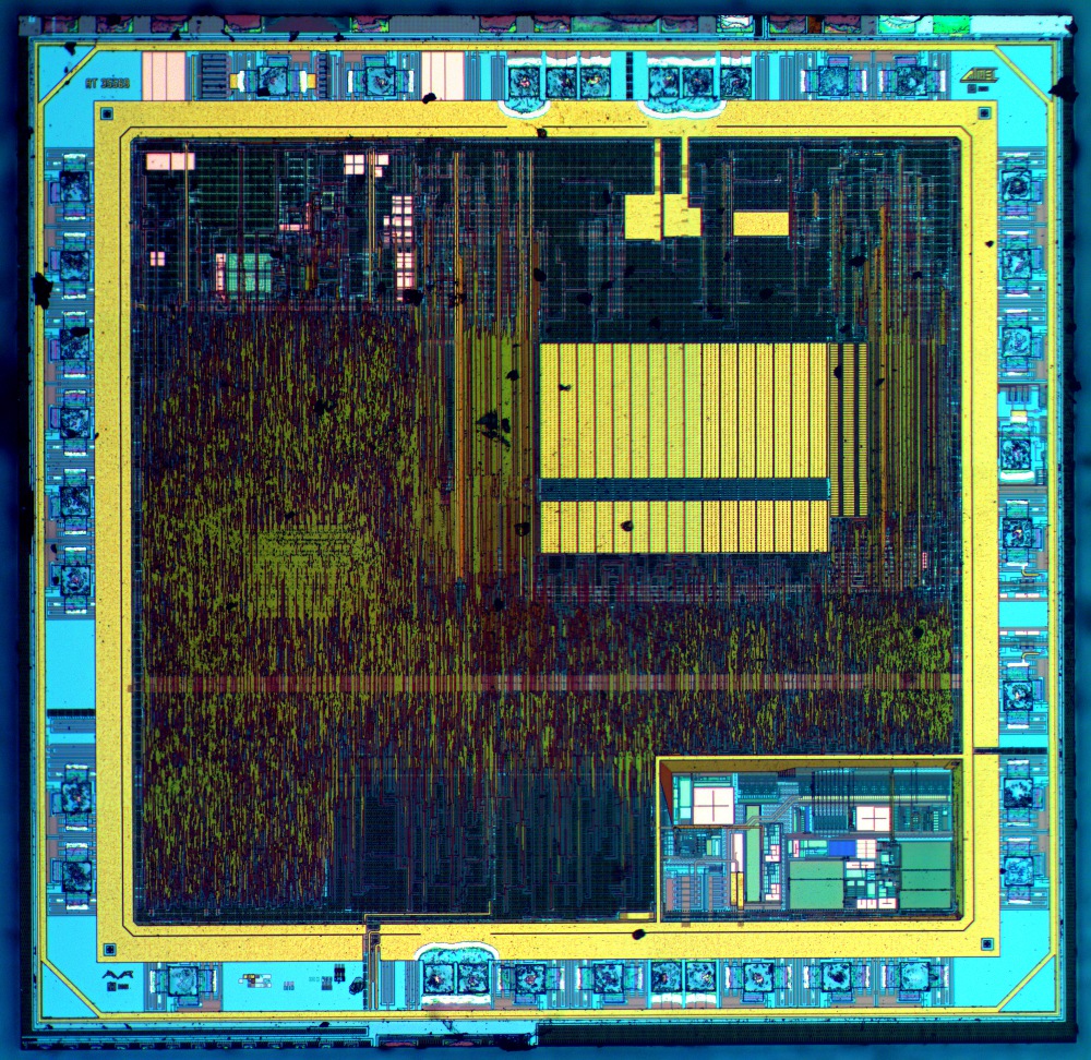
With regards to the technology used on various 8-bit MCUs, you just have to know where to look. Zeptobars.ru has loads of IC pictures, including MCUs.

ATmega8 die shot can be found here: http://zeptobars.ru/en/read/atmel-atmega8. It uses 500nm technology, according to the author.

enter image description here

Another page has some more MCUs, including MSP430 and PIC. The PICs are based on 1200nm technology.

EDIT: If you require a more reputable source, then try searching for "<manufacturer> nanometer". As an example, I found this press release from Atmel that says that MCUs will be manufactured using 130nm technology. And here's a page from NXP mentioning 90nm process.

\$\endgroup\$
4
  • 2
    \$\begingroup\$ So the information comes from opening up the chips and measuring it? I cant really quote these sources on an academic work. I was expecting manufacturers to mention this somewhere in one of their million manuals and application notes... \$\endgroup\$
    – AmiguelS
    Commented Jan 3, 2016 at 19:25
  • \$\begingroup\$ I don't think you'll find this in a manual, as it is not relevant most of the time. Maybe you could find some info about the manufacturer's fabs in some about page, but even then, they may use different technologies for different chips. \$\endgroup\$
    – Armandas
    Commented Jan 3, 2016 at 19:28
  • 1
    \$\begingroup\$ @AmiguelS updated my answer with an Atmel PR page as an example. \$\endgroup\$
    – Armandas
    Commented Jan 3, 2016 at 19:32
  • \$\begingroup\$ @AmiguelS "Actually measuring" sounds academic enough to me... \$\endgroup\$
    – Cedric H.
    Commented Jan 3, 2016 at 23:16
3
\$\begingroup\$

The reasons that (smaller) embedded processors (MCUs) are not built on advanced nodes are cost and performance.

Advanced nodes use very low voltage supplies (e.g. 0.9 V), and interfacing these with 'high' voltage -- e.g. 3.3 V or 5 V peripherals is not trivial; adding this capability to the process would increase the wafer cost.

Wafers in advanced nodes are very expensive, and while an embedded processor (MCU) would be very small, the periphery around it (pads for bonding the wires, space for separating the ICs) would be a relatively large portion, and therefore the total cost would likely be higher.

Advanced processes are suitable for very high frequencies (many GHz) -- embedded MCUs do not need that level of performance.

Static leakage current in advanced processes is relatively high (higher than 180 nm processes), and so if an MCU was built in such a process, current consumption would likely be higher.

\$\endgroup\$
0
\$\begingroup\$

Intel and AMD are on the cutting edge of CMOS process development. They advertise their process nodes (which are not necessarily the same as gate lengths) to show off their progress. 8-bit microcontrollers use ancient (cheap) process nodes, so there's no point in bragging about them.

When you buy an Intel CPU, Intel has done the design and manufacturing. Microcontrollers and other embedded processors often use a mix of off-the-shelf and in-house design. ARM CPUs are a prominent example. The MCU company (TI, in this case) licenses HDL code for the CPU from ARM, then incorporates it into a larger design. The HDL is then synthesized into a netlist targeted at a specific process node and its cell library. It's up to the MCU company to decide which process node to use, and whether to manufacture in-house or at a foundry. The decision is made based on requirements for performance, power consumption, and cost. Newer processes have larger up-front costs. So as a rule of thumb, the company whose logo is on the chip decides which process node to use.

Since embedded hardware is less focused on maximum performance, the process node is often unmentioned in IC documentation. If you want citable sources, look at articles from industry news outlets. For example, this article says that the AM335x chip on the BeagleBone Black is made in a 45nm process. You could also contact the company directly. They might have an archive of press releases you could cite.

\$\endgroup\$

Your Answer

By clicking “Post Your Answer”, you agree to our terms of service and acknowledge you have read our privacy policy.

Not the answer you're looking for? Browse other questions tagged or ask your own question.