0
\$\begingroup\$

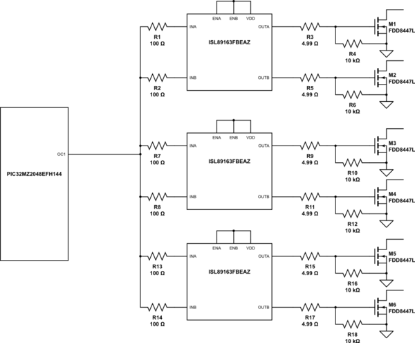
I am using a PIC32MZ's OC pins (PWM mode, fault disabled) as input to a dual MOSFET driver (ISL89163 A). I need one OC pin to drive 3 drivers i.e 6 inputs each. The pulse width would be around 100~150ns with a repetition frequency around 50~100Hz. The PIC's datasheet ( http://ww1.microchip.com/downloads/en/DeviceDoc/60001191E.pdf page 565) says each I/O pin should be able to source/sink 25mA. I found quiescent current graphs on the driver's datasheet but I am not sure how much its input pins would need. How do I calculate the input current needed by the driver and make sure the PIC pins would be able to source it? Using separate OC pins for each driver is not an option since I am doing something similar on the remaining OC pins too. Also, it's a requirement that each of the 6 inputs shown below are roughly the same, so I do not want to go into synchronizing the OC outputs if I use separate OC pins. I am using FDD8447L for the MOSFET. Here's what my circuit roughly looks like now:

EDIT: Should have noticed the 10uA input bias current specified on the ISL89163 datasheet earlier, dunno how I missed it. Anyway, does that mean the PIC OC pin needs to be able to source/sink only 60uA (10uA x6) of current. How do my input 100ohm resistors affect this?
schematic

simulate this circuit – Schematic created using CircuitLab

\$\endgroup\$
1
  • \$\begingroup\$ One PIC pin can drive all 6 inputs. The 100 ohms resistors if all placed near the PIC may slow down the edge rate of the signal a little. Unless you have identified a reason for them to be there, you don't need them. \$\endgroup\$
    – rioraxe
    Commented Apr 13, 2016 at 4:47

1 Answer 1

1
\$\begingroup\$

Correct -- the spec to look for is the input-bias current of the parts you are trying to drive, and in this case, the datasheet specifies they are 10uA each. I initially thought that indicated BJTs, but the datasheet makes it clear they are FET input stages (high impedance).

Assuming your PIC is running at 3.3V, those 100R resistors will be fine and not affect the ability of your device to source the current required for the drivers. From a DC point-of-view, I think you are OK.

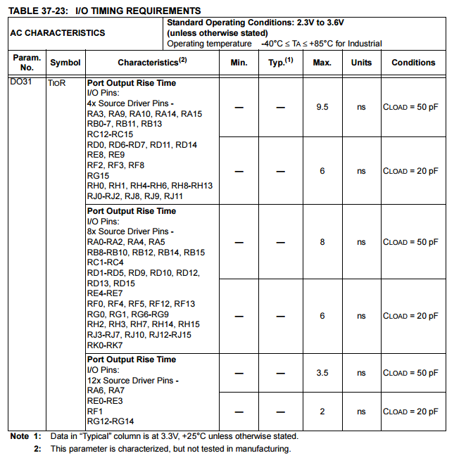
Here is the thing that wigs me out about that circuit schematic though -- you are driving a relatively low frequency signal into six separate devices in a fan-out configuration. It appears the rise-time of the PIC outputs are fairly slow:

enter image description here

And the total input capacitance of the devices you're driving appears to be 2pF * 6 = 12pF + some stray trace capacitance which still puts you (probably) under 20pF. How long are the trace lengths we are talking here? There is the possibility (unlikely with how slow those drivers are) of getting reflections which could lead to double-triggering those drivers, though they do have Schmitt triggers to improve noise-rejection / tolerate slow-rising signals.

The safest thing to do IMO is to buffer the signal to drive all six drivers, but if you can prove via design that it's not necessary to do so due to the way you layout the traces (fly-by routing with small stubs, for instance), that's also fine and you'll save on BOM cost and part count.

You should answer (since I can't tell from your provided info yet):

  1. Is there any possibility I'm going to end up with more than 25pF (or so) of capacitive loading?
  2. Does my PCB layout result in a trace with long stubs or otherwise weird routing that requires me to consider the rise-time / reflections occuring?
\$\endgroup\$
2
  • \$\begingroup\$ Thanks, I hadn't thought of this. The issue here is to do a proof of concept, I'm using a PIC eval board ( ww1.microchip.com/downloads/en/DeviceDoc/70005230B.pdf ) and the rest of the circuitry would be in a separate board. The traces from the input resistors to connectors on the edge of the board would be pretty short (a few mm) but connecting the eval board to the actual board with jumper cables would be an issue. Any suggestions for cables I can use to minimize this? \$\endgroup\$
    – Manu
    Commented Apr 12, 2016 at 18:48
  • \$\begingroup\$ I think for a breadboard-like setup you will "probably"(TM) be fine -- just make sure for the cable that you have a nice-sized ground / signal return path to minimize cross-talk / loop area. Lots of conductors will lower resistance for DC, placing grounds adjacent to signals (if a ribbon cable) will help with AC return. \$\endgroup\$ Commented Apr 12, 2016 at 19:00

Your Answer

By clicking “Post Your Answer”, you agree to our terms of service and acknowledge you have read our privacy policy.

Not the answer you're looking for? Browse other questions tagged or ask your own question.