30
\$\begingroup\$

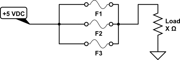
When I went to school we had some basic circuit design and stuff like that. I learned that this was a bad idea:

schematic

simulate this circuit – Schematic created using CircuitLab

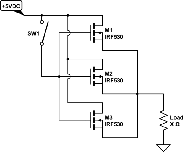
Since the current will almost certainly not flow equally over these three fuses. But I have seen multiple circuits that uses parallel transistors and MOSFETs, like this:

schematic

simulate this circuit

How does the current flow through these? Is it guaranteed to flow equally? If I have three MOSFETs that each can handle 1 A of current, will I be able to draw 3 A of current without frying one of the MOSFETs?

\$\endgroup\$
8
  • 1
    \$\begingroup\$ You basically have 3 NMOS in parallel. Assuming they're all 100% equal and at the same temperature, then yes the current will divide so each takes 1/3 of the total. But operated like this, the NMOSes will not work as switches but as source followers and will drop about 2 to 3 V. \$\endgroup\$ Commented Dec 12, 2016 at 16:01
  • 3
    \$\begingroup\$ FYI - Connecting fuses in parallel is dangerous. Wiring should be protected with one fuse. \$\endgroup\$
    – vofa
    Commented Dec 12, 2016 at 16:02
  • 3
    \$\begingroup\$ I realize you ask this regarding the current distribution between them, but if you ever paralell MOSFETs like this, you must use individual gate resistors or you will have destructive oscillations. \$\endgroup\$
    – winny
    Commented Dec 12, 2016 at 20:24
  • 3
    \$\begingroup\$ @vofa The question asker knows that. It says so in the second sentence. \$\endgroup\$ Commented Dec 12, 2016 at 21:02
  • 1
    \$\begingroup\$ I understand that. I just wanted to add this for any future endeavorer who might try it or put it in production like we did. Ouch! So many returns. \$\endgroup\$
    – winny
    Commented Dec 12, 2016 at 21:13

6 Answers 6

37
\$\begingroup\$

MOSFETs are a bit unusual, in that if you connect several of them in parallel, they share the load quite well. Essentially, when you turn on the transistor, each one will have a slightly different on-resistance and a slightly different current. The ones carrying more current will heat up more, and increase their on-resistance. That then redistributes the current a bit. Provided the switching is slow enough for that heating to happen, it gives a natural load-balancing effect.

Now, the natural load-balancing isn't perfect. You'll still end up with some imbalance. How much will depend on how well matched the transistors are. Several transistors on one die will be better than separate transistors, and transistors of the same age, from the same batch, or which have been tested and matched up with a similar one will help. But as a very rough number, I'd expect you to be able to switch about 2.5A with three 1A MOSFETs. In a real circuit, it would be wise to look at the manufacturer's datasheets and application notes to see what they recommend.

Also, that circuit is not quite what you want. You'd be better off using the N-type MOSFETs for low-side switching. Or, if you want to stick with high-side switching, get some P-type MOSFETs. You will also need an appropriately placed resistor to make sure the gates are not floating when the switch is open.
\$\endgroup\$
6
  • 1
    \$\begingroup\$ Its perhaps worth adding that the circuit will need a gate discharge resistor. Where it goes depends on whether you're using N or P channel MOSFETs. \$\endgroup\$
    – Steve G
    Commented Dec 12, 2016 at 16:47
  • \$\begingroup\$ Good point. Edited. \$\endgroup\$
    – Jack B
    Commented Dec 12, 2016 at 16:49
  • \$\begingroup\$ This is just a simplified example circuit to illustrate what I was asking. This is not going to be used in real life. \$\endgroup\$ Commented Dec 12, 2016 at 19:28
  • \$\begingroup\$ I get a bit confused reading your answer, as it mixes the term "mosfet" with "transistor". To me, mosfets (nmos and pmos) are different to transistors (npn and pnp). \$\endgroup\$
    – K.Mulier
    Commented Aug 2, 2017 at 7:53
  • 3
    \$\begingroup\$ MOSFET stands for Metal Oxide Field Effect Transistor. The term for npn and pnp transistors is Bipolar Junction Transistor (BJT). I think the common usage of the word "transistor" includes MOSFETs, BJTs, JFETs as well as more esoteric things like tunnelling transistors, nanowire transistors and single electron transistors which rarely appear in consumer electronics. \$\endgroup\$
    – Jack B
    Commented Aug 2, 2017 at 9:08
13
\$\begingroup\$

International Rectifier - Application Note AN-941 - Paralleling Power MOSFETs

Their "In-summary" (emphasis added):

  • Use individual gate resistors to eliminate the risk of parasitic oscillation.
  • Ensure that paralleled devices have a tight thermal coupling.
  • Equalize common source inductance and reduce it to a value that does not greatly impact the total switching losses at the frequency of operation.
  • Reduce stray inductance to values that give acceptable overshoots at the maximum operating current.
  • Ensure the gate of the MOSFET is looking into a stiff (voltage) source with as little impedance as practical.
  • Zener diodes in gate drive circuits may cause oscillations. When needed, they should be placed on the driver side of the gate decoupling resistor(s).
  • Capacitors in gate drive circuits slow down switching, thereby increasing the switching unbalance between devices and may cause oscillations.
  • Stray components are minimized by a tight layout and equalized by symmetrical position of components and routing of connections.
\$\endgroup\$
13
\$\begingroup\$

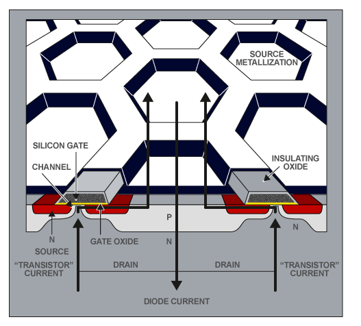
Note that MOSFETs rely on equal current distribution even on the single-device scale. Unlike theoretical models where the channel is represented as a line between source and drain, real devices tend to distribute the channel region over the die to increase maximum current:

enter image description here

(channel region is distributed under hexagonal pattern. the picture is taken from here)

Parts of the channel can be thought of as separate MOSFETs connected in parallel. Current distribution in parts of the channel is close to uniform thanks to the natural load-balancing effect @Jack B described.

\$\endgroup\$
2
  • \$\begingroup\$ Note that this image is actually of a bipolar power transistor, not a MOSFET. Compare with the photo closer to the top of the page, which is a HEXFET. The structural differences are subtle, but note that the gate bonding wire connects to a thin stripe of metallization around the perimeter of the die. \$\endgroup\$
    – Dave Tweed
    Commented Dec 13, 2016 at 15:08
  • 1
    \$\begingroup\$ @DaveTweed It seems I somehow associated the word complimentary with CMOS, and CMOS with MOSFET. Hopefully the new image is more on-topic. \$\endgroup\$ Commented Dec 13, 2016 at 16:57
12
\$\begingroup\$

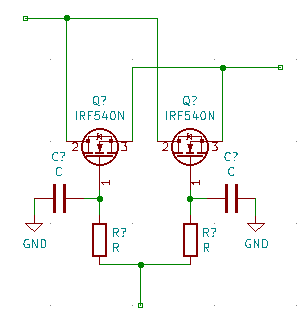
Nearly 3 years later, for the benefit of anyone finding this now... The question was answered very well, but I would also add that parasitic oscillation can be an issue if the gates are just tied together directly. Generally, you'll see a simple RC net at the gates to prevent it. Like so.

Mosfets in Parallel

The values can be pretty low; typically 470ohm Rs and 100pF Cs

\$\endgroup\$
1
\$\begingroup\$

One of the tips given was: - Ensure that paralleled devices have a tight thermal coupling. However, I think the automatic load balancing caused by the positive temperature coefficient of resistance, will work better without tight thermal coupling! In a buck-converter, you may also have schottky diodes in parallel. Their thermal coefficient works the other way. Their forward voltage loss will decrease with rising temperature. So, for those, tight thermal coupling is very important. Otherwise the current in the hottest diode may run away!

\$\endgroup\$
0
\$\begingroup\$

I think the easiest way to look at this problem is to look at the drain to source resistance on the data sheet. Worst case is when you have one device at the lowest on resistance and the rest at the highest resistance. It is just a simple parallel resistance problem to calculate how much current will be flowing through each transistor. Just keep in mind, when selecting a device to give yourself some guardband to account for temperature variation and effects of aging from the device.

\$\endgroup\$
1
  • 1
    \$\begingroup\$ This is not a high-quality answer, and it adds nothing to what other answers have already said. You completely neglect important effects such as the positive temperature coefficient of resistance, which provides the self-balancing action that others have mentioned. \$\endgroup\$
    – Dave Tweed
    Commented Dec 13, 2016 at 15:13

Your Answer

By clicking “Post Your Answer”, you agree to our terms of service and acknowledge you have read our privacy policy.

Not the answer you're looking for? Browse other questions tagged or ask your own question.