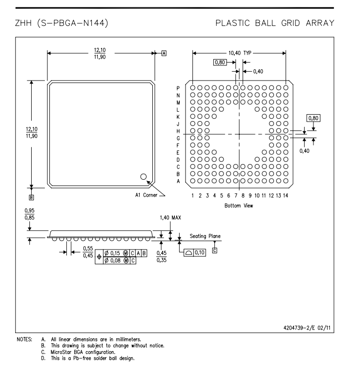
I wanted to become more familiar with BGA package PCB design and have selected a chip to learn with. This is a Texas Instruments DSP here. I've studied several 'BGA at home' guides and believe to have an understanding of what is required for design and assembly.
However, it seems like this chip requires very small traces compared to chips used in several guides I've read. This BGA package has a pitch 0.8mm and 0.55mm ball diamater. The resulting width between balls is ~10 mils. This seems like a pretty unfortunate pitch to ball diameter ratio.
I haven't even gotten to the assembly portion yet and this seems like it will be difficult to get a PCB printed that satisfies this spec.
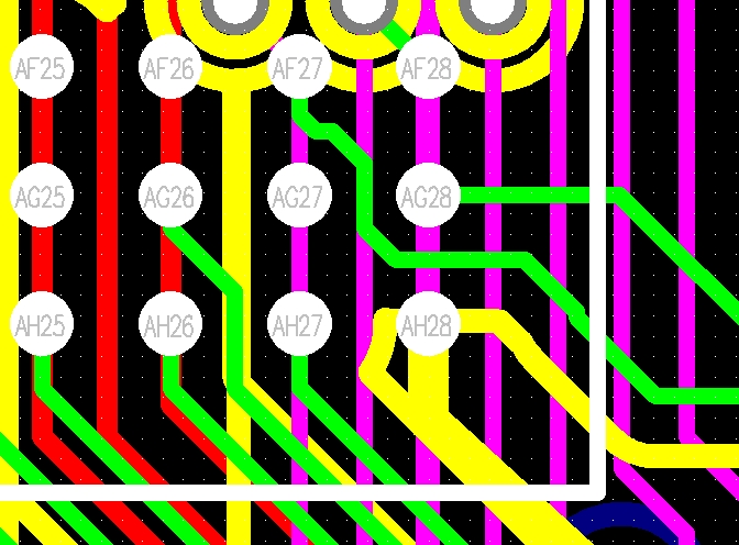
My question: What is the recommended PCB trace width for navigating this 10mil gap?
How would a manufacturer do this? It seems like anything smaller than the typically 5 mil trace width would add further costs.
BGA footprint provided below:


