1
\$\begingroup\$

I tested an amplifier on a circuit board with a network analyzer. It was tested under input power of -20dBm, which is well within the linear region.The amplifier uses SMA connectors.

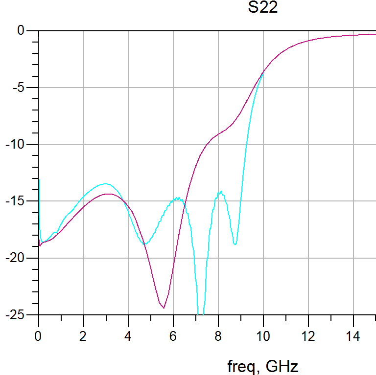
The simulated return loss S22 is smooth, but S22 of the fabricated die shows ripples at round 7GHz. The red trace is from simulation, and blue trace is from measurement.

Do anyone have idea why it might happen? Probably something to do with the RF connectors?

Thanks!!

enter image description here

\$\endgroup\$
6
  • 1
    \$\begingroup\$ We can't read your mind. What kind of device is it? What is the equivalent circuit of its output? How did you package it? What kind of connectors did you use? Or what kind of microprobes? How did you power it during the test? What kind of calibration did you use? What are the two different curves on the chart? \$\endgroup\$
    – The Photon
    Commented Apr 7, 2017 at 21:54
  • \$\begingroup\$ I edited the question. hopefully gives you more info. \$\endgroup\$ Commented Apr 7, 2017 at 22:03
  • \$\begingroup\$ How long is the trace between the connector and the amplifier chip? How carefully was the PCB designed? What materials is the PCB made out of? A photo of the PCB might help us spot an issue, also. \$\endgroup\$
    – The Photon
    Commented Apr 7, 2017 at 22:16
  • \$\begingroup\$ Full calibration to test set is key to accurate measurements when I used Anritsu SA in same band for production tests. Your dielectric loss tangent and controlled impedance design and quality of SMA connectors will all affect this. The Die has 3GHz more bandwidth using -13dB criteria ( usually -15dB is desired) The dips are all phases of impedance shifts of excited wave of "almost" equal distributed inductance and capacitance. Yours rises sharply at 6.5Ghz which might be improved on with a Smith chart analysis, check all port connector quality and redo Short/open match calibration. \$\endgroup\$
    – D.A.S.
    Commented Apr 7, 2017 at 22:31
  • \$\begingroup\$ Hopefully not Pasternack SMA's unless certified \$\endgroup\$
    – D.A.S.
    Commented Apr 7, 2017 at 22:34

1 Answer 1

1
\$\begingroup\$

The simulated return loss S22 is smooth, but S22 of the fabricated die shows ripples

What that means is that what you are measuring is not what you simulated, period. The difference between them can be interpretted to hint to you which part of the model is wrong.

What you simulated is probably a perfect network analyser, connected by perfect 50ohm line through perfect connectors, to a circuit which is modelled exactly correctly.

A common problem is a length of line that's the wrong impedance, or line between two connectors each of which has a reflection, connecting the ana to the device. This will set up an error which is periodic in frequency, with a period related to half the line length.

If you calibrate the measurement system to a reference plane within your test piece, this will mostly take out the influence of the ana, the connecting line, and up to connector repeatability, the connectors.

The difference in modelled and actual traces suggests a ripple that does not look periodic, suggesting to me that it's not such a line resonance. It does however look suggestive of the increasing frequency of ripple that one gets as one approaches the corner frequency of a high order filter. Perhaps you have some big unmodelled L and C equivalents somewhere, for instance where the transmission line changes profile.

If you have suitable software on your ana, you might try to simulate a TDR view of the difference. This will show you a time domain interpretation of the impedance errors which might hint to where the major deviation is.

\$\endgroup\$

Your Answer

By clicking “Post Your Answer”, you agree to our terms of service and acknowledge you have read our privacy policy.

Not the answer you're looking for? Browse other questions tagged or ask your own question.