2
\$\begingroup\$

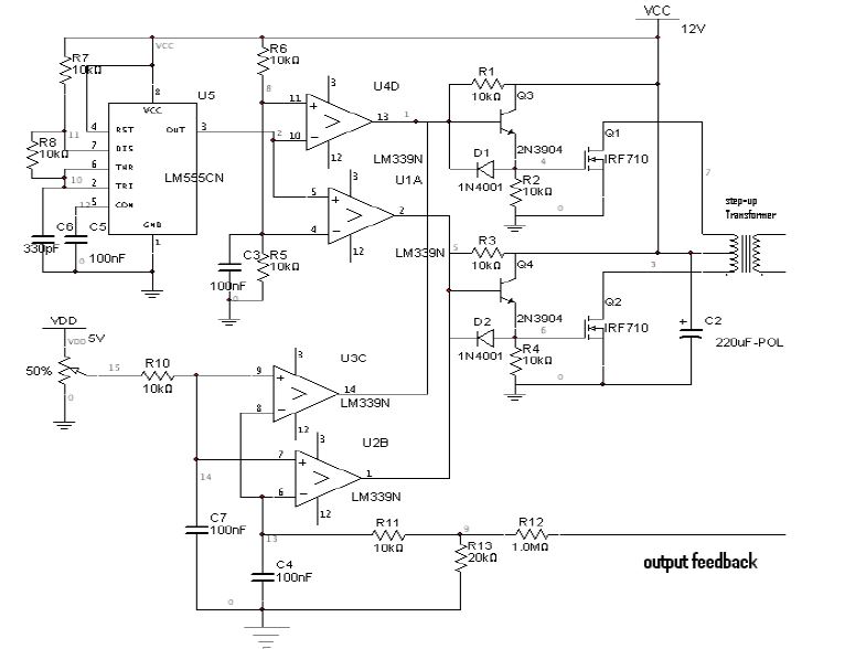
This is a circuit for switching the transformer at high frequency and so that we get ac on the secondary side. A voltage multiplier circuit is connected to the secondary of the transformer which will give a high voltage dc at the output. That dc voltage is then fedback which is shown in the figure as OUTPUT FEEDBACK. In this circuit i am not able to understand

  1. the use of 220microFarad capacitor which is connected with the centre tap of the transformer

  2. How is feedback circuit working, Is it a window comparator circuit?

  3. Use of transistor, I mean the Square wave which we are getting can be directly fed to the Mosfet but why have we used transistors?

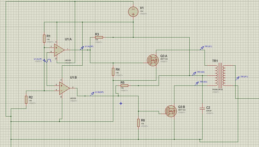
    1. I have uploaded a photo in reference to my 3rd question. I have simply removed transistors in this and i did its simulation in proteus and is working. I am unable to understand the use of transistor in this??new circuit

enter image description here

\$\endgroup\$

4 Answers 4

2
\$\begingroup\$
the use of 220microFarad capacitor which is connected with the centre tap of the transformer

This reduces ripples in the power supply. Current is drawn from the 12 V supply in pulses. C2 reduces the impedance of the supply at the switching frequency, thereby reducing the voltage excursions caused by the current pulses.

How is feedback circuit working, Is it a window comparator circuit?

No, it's a plain old comparator circuit, just that there are two of them. Note that each of the comparators U3C and U2B have the same inputs. They will therefore produce the same outputs. The positive input comes from a reference voltage produced by the pot labeled "50%", then filtered by R10 and C7. This is meant to be a fixed DC level, adjusted so that ultimately the desired DC level is achieved after rectifying the transformer output.

I haven't looked it up, but from the circuit it seems clear that the comparators have open collector outputs. Multiple comparators with outputs wired together therefore perform a AND function. The comparators U4D and U1A produce pulses of opposite polarity to ultimately drive the push-pull switching elements. The outputs of U3C and U2B simply ground these signals, thereby keeping the switches off, when the feedback signal is above the threshold.

Use of transistor, I mean the Square wave which we are getting can be directly fed to the Mosfet but why have we used transistors?

This question makes no sense since MOSFETs are transistors.

The circuitry between a comparator output and its FET gate is a crude FET driver. It takes the open collector output of the comparator and drives the FET gate with it actively in both direction.

When the U4D output goes off, it goes up due to R1. That is at the high impedance of 10 kΩ, which would switch the FET slowly. Q3 is used in emitter follower configuration, and acts as a impedance buffer. It reduces the 10 kΩ drive by its gain. If the gain of Q3 is 100, for example, then the FET gate is being driven high by about 100 Ω instead of the original 10 kΩ.

That works for the rising edge, but does nothing for the falling edge, which would only drive the FET gate low due to R2. D1 fixes this by allowing a direct discharge path for the FET gate charge when the comparator output is actively driven low.

\$\endgroup\$
1
  • \$\begingroup\$ I have uploaded a photo in reference to my 3rd question. I have simply removed transistors in this and i did its simulation in proteus and is working. I am unable to understand the use of transistor in this?? link to the circuit is: i.sstatic.net/Jso6s.jpg \$\endgroup\$ Commented Jun 1, 2017 at 9:18
2
\$\begingroup\$

This circuit has too much problems, don't try to build it unless you want to spare couple of weeks and burn a bunch of parts.

How it works:

555 is connected as astable square wave generator. For proper operation its duty cycle should be exactly 50%, but with given component values it wont happen. It will be something like 66% / 33%. The problem here is that one of the power transistors will work 66% of the time, and the other the rest 33%. This will cause unballanced operation of the HF transformer which limits its power capabilities to a much lower value.

U1A and U4D (it should be U1D) form an invertor so non-inverted pulses are passed to Q2 and inverted to Q1. Also this stage should provide some "dead-time" - time when both MOSFETs are off. This is not done here. The problem is that the second MOSFET turns on before the first is fully turned off. This causes very large current to flow trough both transistors during switching. The overwall efficiency will be much lower and MOSFETs will overheat.

Q3 with its surrounding parts and for a gate driver for Q1, which is probably the only thing that will work fine in this schematic. Same for Q4 - driver for Q2.

U3C, U2B - the are not connected as window comparators, they are separated parts to pull down two separate drive signals when output voltage divided by R12/R13 is higher than reference voltage of the potentiometer. This is a lesson how a feedback should not be made. Device operation will be very poor. A proper SMPS feedback uses an Error Amplifier (OpAmp) often with limited gain (both DC and AC) and its output signal is compared to a sawtooth waveform produced by an oscillator or by switching current. This approach gives a more stable operation because each period the duty cycle is chahged just a little. In the proposed circuit feedback comparators will skip pulses and also it can jump into situation where every second pulse is missed, causing the supply to work as a single transistor forward converter, not a push-pull. This would overheat or even saturate transformer and overheat (one of) the transistors.

I doubt that this circuit was ever built or if so its operation was far from optimal.

Directly to your questions:

  1. C2 is needed to provide a good low impedance path for the inverter (transformer stage). It is OK there, maybe its value should be raised depending ot output power.

  2. It is not a window comparator. See above. It will work very poor, it will make the inverter to skip pulses and create awful audible noise and to overheat.

  3. The ouptut of 555 is low power and if it is passed directly to MOSFET it will not drive them with good waveforms. Also for one of the transistors waveform should be inverterd.

This topology is called "push-pull". You can browse the net to get more detailed explanations on how it works.

\$\endgroup\$
4
  • \$\begingroup\$ .+1 terrible circuit .The 555 is featured on www.badbeetles.com . \$\endgroup\$
    – Autistic
    Commented May 31, 2017 at 11:24
  • \$\begingroup\$ This isn't a great circuit, but calling it "dumb" is going too far. "Simplistic" might be a better description. I've actually seen worse in commercial 12 V DC to 110 V AC inverters for use in motorhomes and the like, and those worked. A PWM generator in a micro would be better, simpler, and provide for dead time. Still, this will work. Killing pulses when the feedback signal is above a threshold really isn't all that bad. Remember, the desired output seems to be DC rectified from the transformer output. This isn't a inverter, where killing the oscillation would be unacceptable. \$\endgroup\$ Commented May 31, 2017 at 11:42
  • \$\begingroup\$ @OlinLathrop thank you. I agree that I shouldn't use such a word. It's my bad, I will edit my phrase. However everything else I wrote is right. This circuit has too much problems and building it is a very bad idea. It conflicts with some of the most importaint power supply design rules like ensuring proper dead time for switches, ballanced transformer magnetization and stable and predictable feedback loop. \$\endgroup\$ Commented May 31, 2017 at 16:40
  • \$\begingroup\$ I added some more explanations for my negative opinion. Updated is in italic. \$\endgroup\$ Commented May 31, 2017 at 16:57
0
\$\begingroup\$
  1. the use of 220microFarad capacitor which is connected with the centre tap of the transformer

That's the best place to put a "smoothing" capacitor given the expected large current surges taken through the transformer primary via the MOSFETs. The idea is to restrict those current surges to where they are needed and not let them propagate long distances through traces or power planes. Standard practice.

  1. How is feedback circuit working, Is it a window comparator circuit??

It looks to me like U3C and U2B restrict the drive levels to the transistors when the output amplitude is reached.

  1. Use of transistor, I mean the Square wave which we are getting can be directly fed to the Mosfet but why have we used transistors?

You MUST use transistors; each leg of the transformer primary must be allowed to "flyback" to twice the supply voltage (voltage at the centre tap). If you drove those transformer legs with a square wave you would convert the flyback energy to heat in the square wave drivers. Imagine the primary as a see-saw. The centre tap is at (say) 12 volts and if you pulled one end down to 0 volts, the other end has to be allowed to rise to 24 volts else the see saw would snap in half.

\$\endgroup\$
1
  • \$\begingroup\$ The third question I think is asking: Why are the MOSFETs not directly driven by the comparators outputs? \$\endgroup\$
    – user28910
    Commented May 31, 2017 at 13:41
0
\$\begingroup\$

Lower comparators shut off both the NPN emitter followers if DC out is too high ( from rectified peak AC out) Wired OR open collector comparators out. very slow step load response time.

Looks like this was designed before SMPS chips were invented for inverters

OR shortly after the wheel was invented,... ;)

Very old MOSFETs with high RdsOn. ( Model T's)

\$\endgroup\$

Your Answer

By clicking “Post Your Answer”, you agree to our terms of service and acknowledge you have read our privacy policy.

Not the answer you're looking for? Browse other questions tagged or ask your own question.