0
\$\begingroup\$

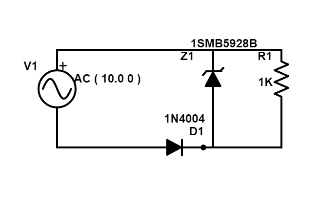
I'm having problem in understanding characteristic of zener diode. In the circuit zener voltage is 5.1V and source voltage is 10V. enter image description here

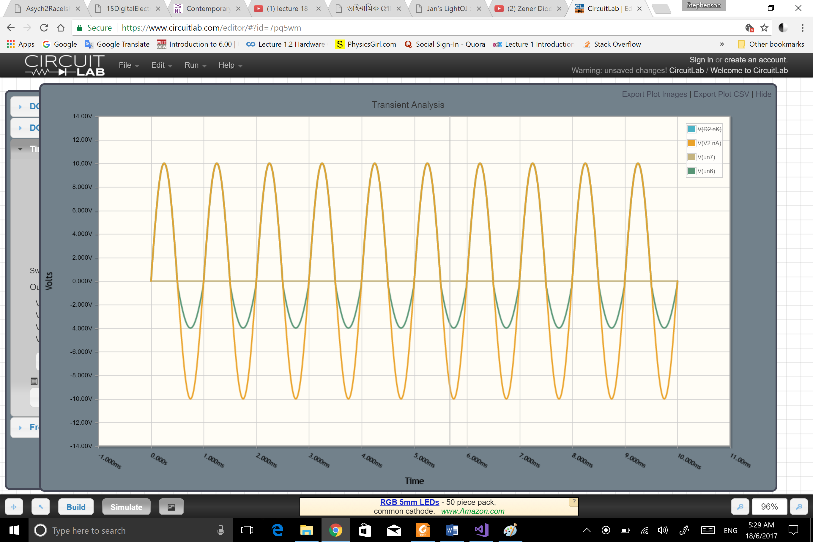
When i simulated in a circuit simulator i got the voltage vs time graph (across the resistance) below where the green wave indicates my output. Can anyone please explain me why i have got this kind of graph? Thanks in advance.

enter image description here

\$\endgroup\$

2 Answers 2

1
\$\begingroup\$

The first thing is to draw your schematic in a way that is easily understood.

Use you common signal at the lower part of the schematic (all your voltages will be referenced to it) and put any components in the upper part of the circuit. In this case you should put the diode in the lead from the positive output of the voltage source.

Wit your current arrangement I don't know where the signal is referenced to - voltages are always one point relative to another.

Also you ALWAYS need a resistor or similar current limiting device in series with a zener to determine how much current flows when you present it with more voltage than the zener breakdown. R1 should be in series with D1 (and D1 is not really necessary, you could replace it with a short circuit).

In a simulation voltage sources are perfect and have zero series resistance. IN your simulation when the voltage exceeds the breakdown of the zener a large current will flow but the voltage source will not be affected.

\$\endgroup\$
1
  • \$\begingroup\$ See my edits - redraw your schematic and it will be more easily understandable \$\endgroup\$ Commented Jun 18, 2017 at 0:17
1
\$\begingroup\$

Assuming that your circuit ground is on the lower end of the AC voltage source, and the sense point is the anode of the zener, then the response can be divided into two sections: positive and negative half-cycles of the AC.

For positive cycles - since D1 is reverse-biased, no current can flow, and the voltage on the zener is equal to the positive voltage from the AC source.

For the negative cycles - D1 is now forward-biased, and so is the zener. So the voltage becomes the sum of the two, but in a negative sense. I'm surprised that the numeric value is 4 volts peak, but I suspect that the fact that there is no current-limiting resistor allows enormous currents in the simulator. I suggest you check.

In order to do what I think you want to do, change your circuit to
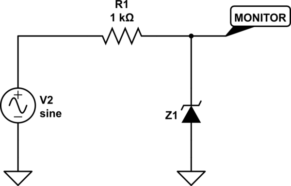
schematic

simulate this circuit – Schematic created using CircuitLab
\$\endgroup\$

Your Answer

By clicking “Post Your Answer”, you agree to our terms of service and acknowledge you have read our privacy policy.

Not the answer you're looking for? Browse other questions tagged or ask your own question.