1
\$\begingroup\$

I built circuit shown bellow (NPN BJT):
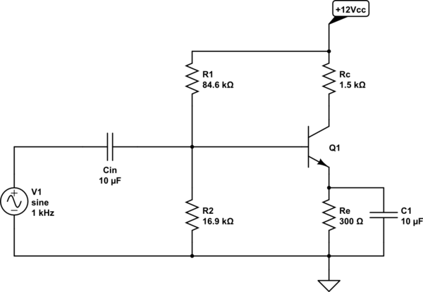
schematic

simulate this circuit – Schematic created using CircuitLab

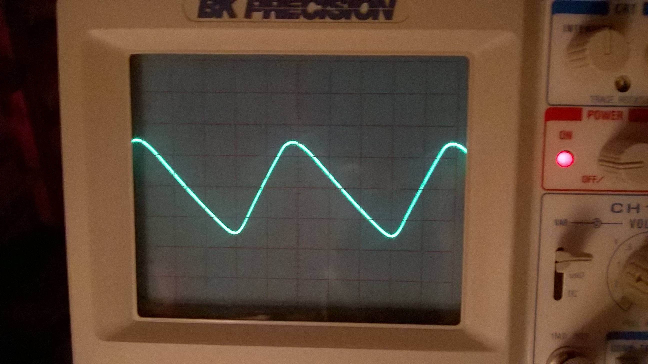
Everything worked normal as it should (except of unwanted distortion). There is that one strange thing I'm seeing lately when I connect oscilloscope's probe between emitter and ground. It is the amplitude of the signal measured - when the amplitude of F.G. is some mV, the emitter amplitude more or less follows the input amplitude measured between base and ground; things change when the input voltage is increased for few 10mV, where the emitter's amplitude looks like this:

enter image description here

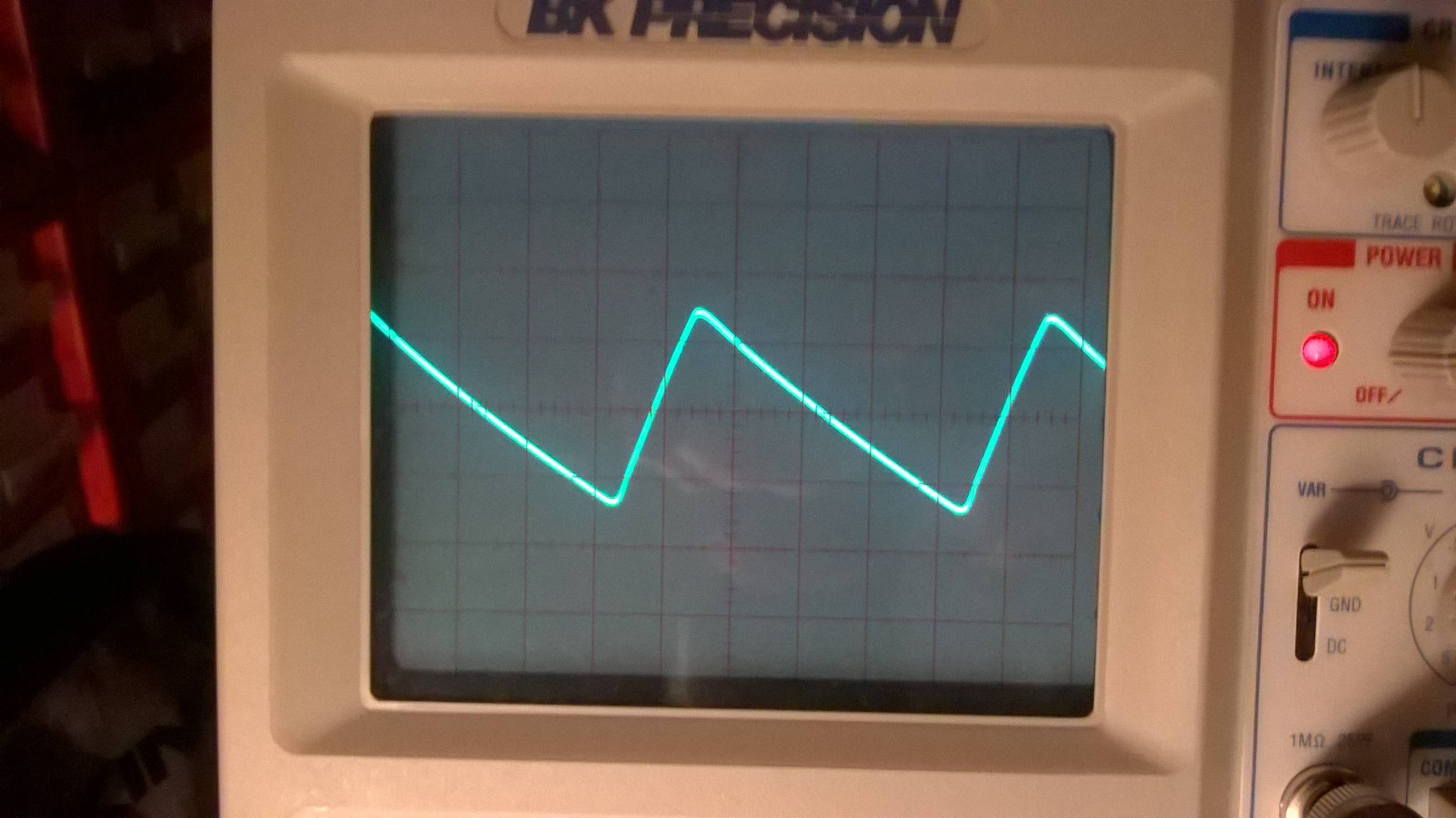
Eventually proceeding to more sharp shape of peak.

enter image description here

Even stranger thing is that, after those triangular waves are shaped, the voltage simply stops at this point as the input voltage is increased.

  • Does this behavior has to do anything with almost constant Vbe which is approx. 0.7V?

  • Or is this another unwanted distortion produced by transistor?

\$\endgroup\$
7
  • \$\begingroup\$ No, has nothing to do with Vbe = 0.7 V. Why would it ? It has everything to do with you overdriving this circuit. The cap on the emitter shorts the emitter to ground for AC-signals this results in a large gain. This means that if you do not want the circuit to distort then you should feed it a small signal. Apply a sinewave of 10 mV or less at the input and look at the voltage on the collector. It should be a sinewave as well. If it is not you're overdriving the circuit and it will distort. \$\endgroup\$ Commented Sep 8, 2017 at 20:43
  • \$\begingroup\$ @Bimpelrekkie At the point where emitter amplitude starts going into triangular shape, the Vce amplitude is still undistorted. \$\endgroup\$
    – lucenzo97
    Commented Sep 8, 2017 at 20:49
  • \$\begingroup\$ @Bimpelrekkie Why would it? because at one point voltage of emitter just stops increasing as the input voltage on the base is increased - don't you find this a bit strange? \$\endgroup\$
    – lucenzo97
    Commented Sep 8, 2017 at 20:51
  • \$\begingroup\$ Read this post: electronics.stackexchange.com/questions/328285/… \$\endgroup\$
    – dirac16
    Commented Sep 8, 2017 at 20:55
  • \$\begingroup\$ I remember you posting earlier about a "simple" amplifier: electronics.stackexchange.com/questions/321110/… I suppose I should be glad you are back to just a single stage. Are you just throwing parts together? Or was there a design process you could elaborate? What are your goals here? \$\endgroup\$
    – jonk
    Commented Sep 8, 2017 at 21:36

3 Answers 3

4
\$\begingroup\$

It's a bit hard to say, given that we can't see any of the scope settings (vertical or horizontal).

But the waveform you're showing is a characteristic of how the emitter bypass capacitor gets charged and discharged. The charging impedance (through the transistor) is much lower than the discharging impedance (through the resistor). As you drive the base harder, the charging current goes up (faster rise time), but the discharging current cannot change (same fall time).

Bit what this really indicates is that the emitter bypass capacitor is too small for the signal frequency — the voltage should not be changing significantly at all. Either pick a higher signal frequency or use a larger bypass capacitor.

\$\endgroup\$
2
\$\begingroup\$

Impedance of 10uF at 1kHz is about 16 Ohms , and emitter can only pull up, while emitter resistor pulls down. You do the math and scrap this circuit.

1st design by specs with gain, input & output impedance and include your load. 2nd choose a topology that supports these requirements. Then after your analysis , ask yourself a better question.

\$\endgroup\$
-1
\$\begingroup\$

@Bimpelrekkie Why would it? because at one point voltage of emitter just stops increasing as the input voltage on the base is increased - don't you find this a bit strange? – Keno

Wrong DC operating point. Look:

R1 to R2 sets (16.9/84.6)*12=2.4V on the base, or approx 1.8V on emiter. So emiter current would be approx 1.8V / 300 Ohm = 6 mA 6 mA thru 1.5k collector resistor would set 9V over it.

That's only 12V-1.8V-9V=1,2V constant voltage between collector and emiter. Select the correct ratio between the collector and emiter resistors to set the DC operating point in the middle between 12V and 1.8V. (That is approx 5v over collector-emiter)

\$\endgroup\$
3
  • \$\begingroup\$ Sadly you are wrong. Q is just fine where it should be and not how you calculated. \$\endgroup\$
    – lucenzo97
    Commented Sep 9, 2017 at 9:59
  • \$\begingroup\$ You are ignoring the 14kohm Thevenin equivalent resistance of the bias network, which introduces a significant voltage drop when the base current is drawn through it. Assuming ​a beta of 100 and Vbe of 650mV, I get a Q point current of 4mA, with 1.2V across the emitter resistor and 6V across the collector resistor, right about where you want it. \$\endgroup\$
    – Dave Tweed
    Commented Sep 9, 2017 at 11:39
  • \$\begingroup\$ Why did you assume beta of 100? Why not 800? Just because it fits nicely? The OP did not say anything about the beta. He said he's got distortions. And big beta could be the cause as with 800 you are much lower 6V on collector and emitter resistor would be 2 volts or something, leaving almost no room for linear mode. \$\endgroup\$
    – Sergey S.
    Commented Jul 20, 2018 at 22:47

Your Answer

By clicking “Post Your Answer”, you agree to our terms of service and acknowledge you have read our privacy policy.

Not the answer you're looking for? Browse other questions tagged or ask your own question.