I find analog switch usually label the two terminal of the switch channel as "S"(Source) and "D"(Drain). Such as this. I think they are equal in function, either can be used as input or output. So why still use the terminology from MOSFETs?
-
\$\begingroup\$ They are not fully equal. See electronics.stackexchange.com/a/308885/34873 \$\endgroup\$– Joren VaesCommented Sep 13, 2017 at 11:18
-
1\$\begingroup\$ @JorenVaes Yes they are in ICs. Furthermore the bulk is not connected to the source, but to the "lowest potential" in nMOSFET (which might not correspont to the source. Think about the pull-down network of a NAND gate) and "highest potential" for pMOSFET. The source and drain are not fixed: in an nMOSFET the source is the one with the lowest potential, the drain is that one with the highest (opposite on pMOSFETs). \$\endgroup\$– next-hackCommented Sep 13, 2017 at 14:25
-
\$\begingroup\$ @next-hack I said this as a simplification for the OP. As I discuss in my post, reality is much more copmlicated. \$\endgroup\$– Joren VaesCommented Sep 13, 2017 at 14:33
2 Answers
First line of description says:
The ADG1436 is a monolithic CMOS device containing two independently selectable SPDT switches
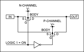
Also, it is worth to see inside.
-
\$\begingroup\$ Yes, I know, they are different in internal. The D is connected to body in NMOS, and S connected to body in PMOS. But when use them, there are any difference? Can't we just use them as a normal switch? \$\endgroup\$– divergerCommented Sep 13, 2017 at 11:57
-
\$\begingroup\$ @diverger The drain is not connected to body! In ICs the body of nMOSFETs is connected to gnd (or Vss), and for pMOSFETs it is connected to Vdd. The pins "S" and "D" in the IC are symmetrical. There is no sense calling them drain or source (some datasheets use S/D_1 and S/D_2). In fact, in an integrated planar nMOSFET, the drain is the terminal connected to the n+ region that has the highest potential. The source is the terminal connected to the n+ region that has the lowest potential (opposite occurs for pMOSFETs). In an t-gate, therefore, S and D function are not assigned a-priori. \$\endgroup\$ Commented Sep 13, 2017 at 14:40
-
\$\begingroup\$ I know the situation in discrete MOSFET. But I may don't understand your figure well. What's the meaning of "BODY" in the figure? It means the V-(+) terminal is the body? \$\endgroup\$– divergerCommented Sep 13, 2017 at 15:31
Different datasheets might have different conventions. Let's consider the famous 4066, which are bilateral switches (Transmission gates).
Here they call each terminal In/Out:
https://www.intersil.com/content/dam/Intersil/documents/cd40/cd4066bms.pdf
Here they call In OR out:
http://www.ti.com/lit/ds/symlink/cd4066b.pdf
Here x and y:
-
\$\begingroup\$ Thanks for your links. I only used analog switches from ADI, so it's maybe ADI's conventions to label them as "S" and "D". \$\endgroup\$– divergerCommented Sep 13, 2017 at 15:19

